Semiconductor structure and forming method thereof
A semiconductor and conductor technology, applied in the field of flash memory, can solve the problems of reducing the reliability and manufacturing yield of memory devices
- Summary
- Abstract
- Description
- Claims
- Application Information
AI Technical Summary
Problems solved by technology
Method used
Image

Examples
Embodiment Construction
[0062] The following describes the present disclosure more fully with reference to the drawings of the embodiments of the present invention. However, the present disclosure can also be realized in various different embodiments, and should not be limited to the examples described herein. The thicknesses of layers and regions in the drawings may be exaggerated for clarity, and the same or similar reference numerals designate the same or similar elements in the drawings.
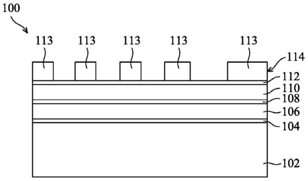
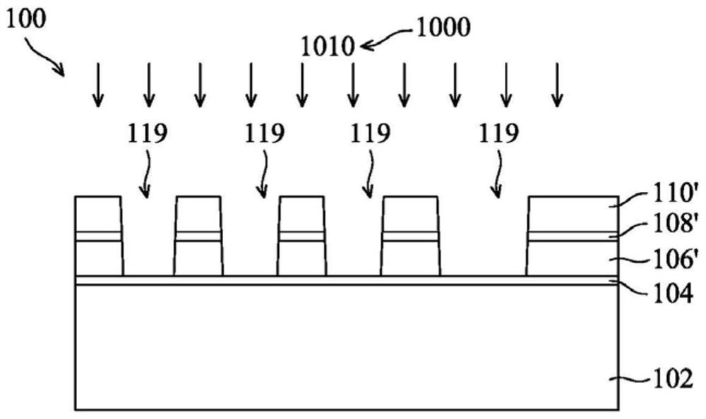
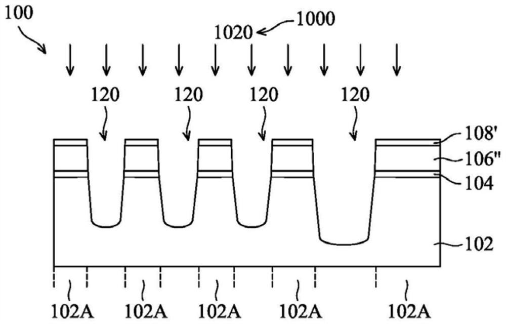
[0063] Figure 1A-Figure 1L According to some embodiments of the present invention, schematic cross-sectional views showing different stages of forming a semiconductor structure are shown. According to some embodiments, a semiconductor structure 100 is provided, such as Figure 1A shown. According to some embodiments, the semiconductor structure 100 includes a semiconductor substrate 102 . In some embodiments, the semiconductor substrate 102 may be an elemental semiconductor substrate, such as a silicon subs...
PUM
 Abstract
Description
Claims
Application Information
 - R&D Engineer
- R&D Manager
- IP Professional
- Industry Leading Data Capabilities
- Powerful AI technology
- Patent DNA Extraction
Browse by: Latest US Patents, China's latest patents, Technical Efficacy Thesaurus, Application Domain, Technology Topic.
© 2024 PatSnap. All rights reserved.Legal|Privacy policy|Modern Slavery Act Transparency Statement|Sitemap