Eureka AIR delivers breakthrough ideas for toughest innovation challenges, trusted by R&D personnel around the world.

Light-emitting diode and manufacturing method thereof

A technology for light-emitting diodes and a manufacturing method, which is applied to electrical components, circuits, semiconductor devices, etc., and can solve problems such as poor current conduction, fracture, and loss of brightness in areas around electrodes.

Inactive Publication Date: 2021-04-09
SHENZHEN INST OF WIDE BANDGAP SEMICON
View PDF7 Cites 6 Cited by
  • Summary
  • Abstract
  • Description
  • Claims
  • Application Information

AI Technical Summary

Problems solved by technology

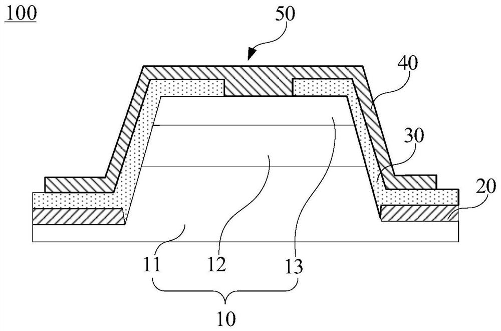
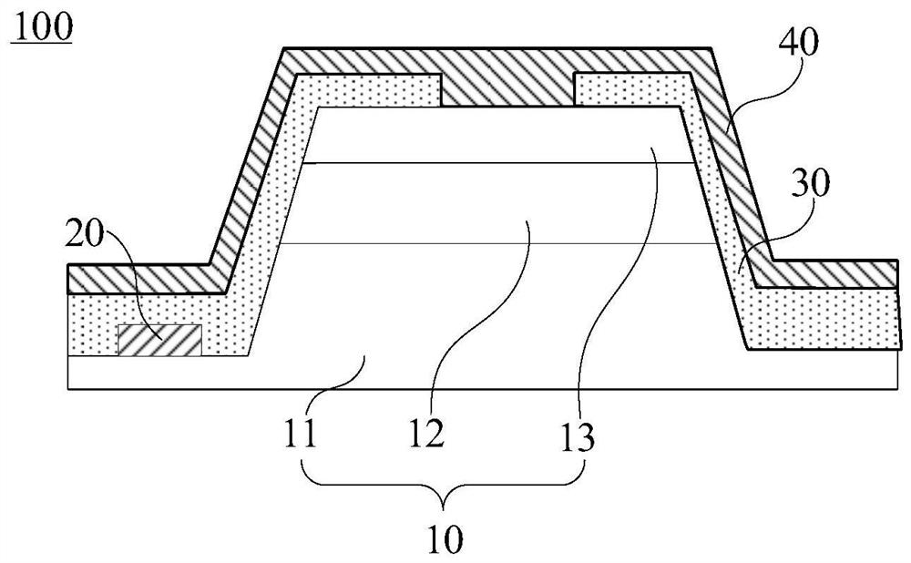
[0003] In the long-term research and development process, the inventors of the present application found that the P and N electrodes of the vertical light-emitting diode with the above structure are located on different sides of the vertical light-emitting diode, and the brightness of the area around the electrodes is seriously lost because the metal electrodes block the light from exiting; in addition, In series-parallel applications, the metal bridges between the vertical light-emitting diodes with the above structure are prone to breakage and metal thinning due to the high step difference due to the wrapping ability, which will lead to poor current conduction or even failure.

Method used


Image

  • Light-emitting diode and manufacturing method thereof
  • Light-emitting diode and manufacturing method thereof
  • Light-emitting diode and manufacturing method thereof

Examples


Embodiment Construction

[0024] The technical solutions in the embodiments of the present application will be clearly and completely described below in conjunction with the accompanying drawings in the embodiments of the present application. Obviously, the described embodiments are only some of the embodiments of the present application, not all of them. Based on the embodiments in this application, all other embodiments obtained by persons of ordinary skill in the art without making creative efforts belong to the scope of protection of this application.

[0025] The terms "first", "second", "third", "fourth", etc. (if any) in the description and claims of this application and the above drawings are used to distinguish similar objects and not necessarily Describe a particular order or sequence. It is to be understood that the data so used are interchangeable under appropriate circumstances such that the embodiments of the application described herein can be practiced in sequences other than those illu...


PUM

PropertyMeasurementUnit
thicknessaaaaaaaaaa
thicknessaaaaaaaaaa

Abstract

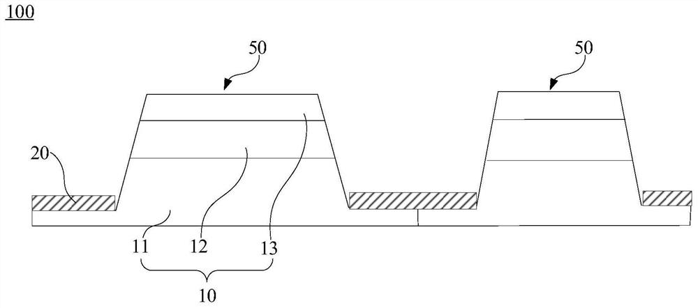
The invention relates to the technical field of semiconductors, and particularly discloses a light-emitting diode and a manufacturing method thereof, and the light-emitting diode comprises an epitaxial layer which comprises a first semiconductor layer, an active layer and a second semiconductor layer which are arranged in a stacked manner; a first electrode layer which is arranged on the exposed first semiconductor layer and is electrically connected with the first semiconductor layer; an insulating layer which covers the first electrode layer and a mesa structure and is provided with a through hole for exposing the second semiconductor layer in the mesa structure; and a second electrode layer which covers the insulating layer so as to be electrically isolated from the first electrode layer and the first semiconductor layer through the insulating layer, wherein the second electrode layer further extends into the through hole so as to be electrically connected with the second semiconductor layer. By means of the mode, the step height difference between the first electrode layer and the second electrode layer can be reduced, the breakage of metal bridges between the light emitting diodes during series-parallel connection application is avoided, and the series-parallel connection structure is more reliable.

Description

technical field [0001] The present application relates to the technical field of semiconductors, in particular to a light emitting diode and a manufacturing method thereof. Background technique [0002] The existing vertical light-emitting diode manufacturing process generally prepares an N-GaN layer, a quantum well layer, a P-GaN layer and a transparent conductive layer sequentially stacked on the growth substrate on the growth substrate, and then bonds the transparent conductive layer and the transparent conductive layer. Support the substrate and peel off the growth substrate, and finally prepare the N electrode on the N-GaN layer. [0003] In the long-term research and development process, the inventors of the present application found that the P and N electrodes of the vertical light-emitting diode with the above structure are located on different sides of the vertical light-emitting diode. Because the metal electrodes block the light from exiting, the brightness of the...

Claims


Application Information

Patent Timeline
Patent Type & Authority Applications(China)
IPC IPC(8): H01L33/38H01L33/00
CPCH01L33/0075H01L33/385
Inventor 朱酉良蒋振宇闫春辉
Owner SHENZHEN INST OF WIDE BANDGAP SEMICON
Why Eureka
Eureka Blog
Learn More