Clock oscillator circuit, charge pump circuit and Flash chip
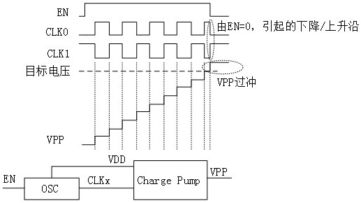
A technology of clock oscillator and charge pump, which is applied in the direction of electric pulse generator circuit and conversion equipment without intermediate conversion to AC, which can solve the problem of charge pump voltage overshoot and so on.
- Summary
- Abstract
- Description
- Claims
- Application Information
AI Technical Summary
Problems solved by technology
Method used
Image

Examples
Embodiment 1
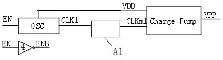
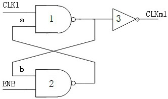
[0032] like image 3 As shown, in some specific embodiments, the level holding module A1 includes a first NAND gate 1, a second NAND gate 2, and a first NAND gate 3, and the first NAND gate 1 of the first NAND gate The input terminal is connected to the first clock pulse CLK output by the clock oscillator OSC, the second input terminal of the first NAND gate 1 is connected to the output terminal of the second NAND gate 2, and the output terminal of the first NAND gate 1 is connected to the first NAND gate. The input terminal of gate 3, the output terminal of the first NOT gate 3 is connected to the input terminal of the charge pump, the output terminal of the first NAND gate 1 is connected to the first input terminal of the second NAND gate 2, and the clock enable EN passes through The logic processing of the seventh NOT gate 4 is input to the second input end of the second NAND gate 2 .
Embodiment 2
[0034] like Figure 4 As shown, in some specific embodiments, the level holding module A1 includes a second NOT gate 5, a third NAND gate 6, a fourth NAND gate 7 and a third NOT gate 8, and the second NOT gate The input terminal of the gate 5 is connected to the first clock pulse CLK output by the clock oscillator OSC, the output terminal of the second NOT gate 5 is connected to the first input terminal of the third NAND gate 6, and the second input terminal of the third NAND gate 6 terminal is connected to the output terminal of the fourth NAND gate 7, and the clock enable EN is input to the second input terminal of the fourth NAND gate 7 after logic processing of the seventh NAND gate 4, and the first input terminal of the fourth NAND gate 7 terminal is connected to the output terminal of the third NAND gate 6, the output terminal of the third NAND gate 6 is connected to the input terminal of the third NOT gate 8, and the output terminal of the third NOT gate 8 is connected ...
Embodiment 3
[0036] Such as Figure 5 As shown, in some specific embodiments, the level holding module A1 includes a first NOR gate 9, a second NOR gate 10 and a fourth NOR gate 11, and the first NOR gate 9 of the first NOR gate The input terminal is connected to the first clock pulse CLK output by the clock oscillator OSC, the second input terminal of the first NOR gate 9 is connected to the output terminal of the second NOR gate 10, and the output terminal of the first NOR gate 9 is connected to the second OR The first input terminal of the NOT gate 10, the clock enable EN is input to the second input terminal of the second NOR gate 10 after the logic processing of the seventh NOT gate 4, and the output terminal of the first NOR gate 9 is connected to the fourth NOT gate. The input terminal of the gate 11 and the output terminal of the fourth NOT gate 11 are connected to the input terminal of the charge pump.
PUM
 Abstract
Description
Claims
Application Information