Supercharge Your Innovation With Domain-Expert AI Agents!

Preparation method of planar TEM sample

A sample and planar technology, applied in the field of planar TEM sample preparation, can solve the problems of reducing TEM test rate and efficiency, spending time and energy, increasing sample preparation time and cost, etc., to improve the preparation success rate and detection efficiency, reduce Production cost and the effect of shortening the production time

Inactive Publication Date: 2021-04-13
GUANGDONG INST OF SEMICON IND TECH
View PDF6 Cites 1 Cited by
  • Summary
  • Abstract
  • Description
  • Claims
  • Application Information

AI Technical Summary

Problems solved by technology

According to the incident angle, incident energy, and thinning time of the argon ion beam, the thinning rate and thinning thickness of the area above the area to be measured A are almost equal to those of other areas of the planar TEM sample 1. Planar TEM sample 1 is uniformly thinned, so it is easy to appear such as figure 2 The situation shown in d that the region A to be measured of the planar TEM sample 1 is completely removed during the final process of argon ion beam thinning is also prone to cause the planar TEM sample 1 to be broken due to the absence of a high-strength wall thickness support
In this way, it is no longer possible to observe and test the planar TEM sample 1, and the prepared sample becomes a waste sample, which requires re-preparation of the sample.
In this case, it takes a lot of time and energy just to prepare the sample, which greatly increases the time and cost of sample preparation, and also reduces the speed and efficiency of TEM testing.

Method used


Image

  • Preparation method of planar TEM sample
  • Preparation method of planar TEM sample
  • Preparation method of planar TEM sample

Examples


no. 1 example

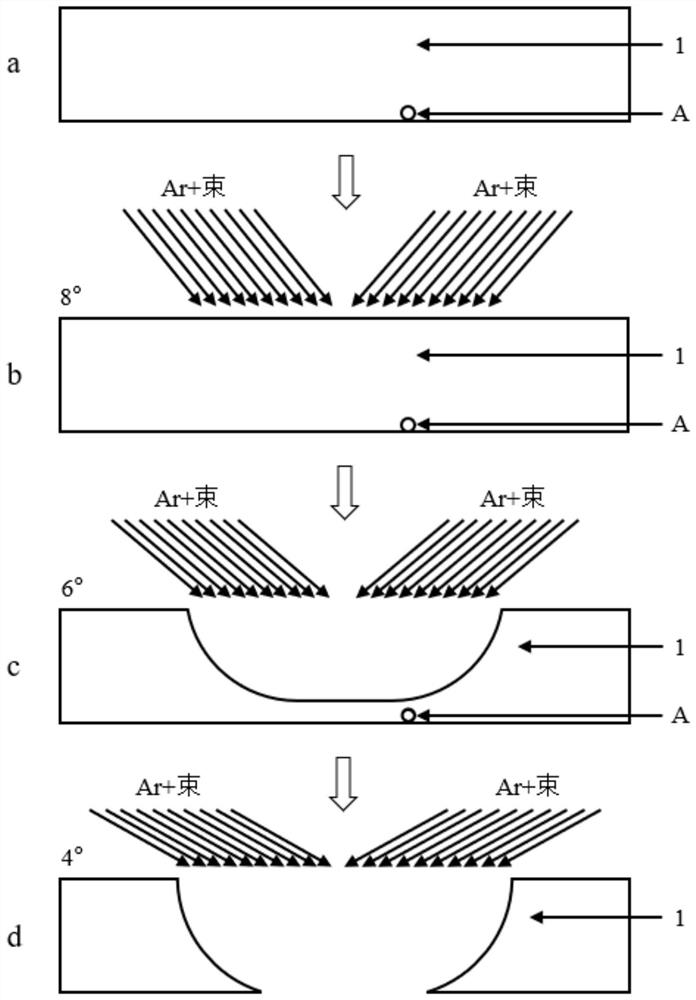
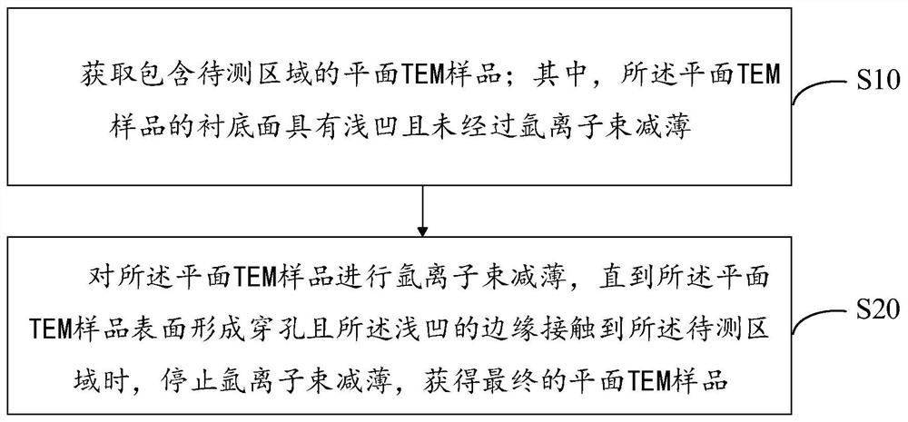
[0036] see image 3 - Figure 7 , a method for preparing a planar TEM sample according to an embodiment of the present invention, at least including the following steps:

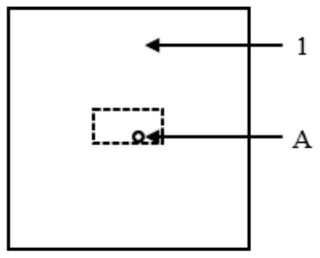
[0037] S10. Obtain a planar TEM sample including a region to be measured; wherein, the substrate surface of the planar TEM sample has a shallow concave;

[0038] It should be noted that in the observation experiment of the transmission electron microscope, the quality of the prepared planar sample directly affects the test results, which is a crucial link in the planar TEM test and analysis process. Using transmitted electrons in TEM to obtain information requires that the prepared planar TEM samples must be very thin, that is, the planar samples are transparent to electrons. Enough electron transmission is required to ensure that the illumination intensity on the screen, charge-coupled device, or photographic film is such that an interpretable planar image can be obtained in a reasonable time. For TEM, t...


PUM

PropertyMeasurementUnit
widthaaaaaaaaaa
surface roughnessaaaaaaaaaa
diameteraaaaaaaaaa

Abstract

The invention discloses a preparation method of a planar TEM sample. The preparation method comprises the following steps that: a planar TEM sample containing a to-be-detected area is acquired, the substrate surface of the planar TEM sample has a shallow recess and is not thinned by an argon ion beam; and argon ion beam thinning is carried out on the planar TEM sample until a through hole is formed in the surface of the planar TEM sample and the edge of the shallow recess is in contact with the to-be-detected area, so as to obtain a final planar TEM sample. According to the method, the shallow recess is formed in the substrate surface of the planar TEM sample; the planar TEM sample with the shallow recess formed in the substrate surface is subjected to argon ion beam thinning, so that the problem that the to-be-detected area on the surface of the planar TEM sample is removed in the thinning process is effectively solved, and the preparation success rate and the detection efficiency of the planar TEM sample are greatly improved; and therefore, the preparation cost of the planar TEM sample is reduced, and the preparation time is shortened.

Description

technical field [0001] The invention relates to the technical field of semiconductor manufacturing, in particular to a method for preparing a planar TEM sample. Background technique [0002] With the development and application of nanotechnology, TEM (Transmission Electron Microscope, referred to as TEM) has increasingly become the main tool for characterizing nanomaterials and devices. It is used to observe the microstructure of materials, such as crystal morphology, Multi-phase crystallization and lattice defects, etc., the point resolution can reach 0.1nm; it is also used to detect the morphology, size and characteristics of thin films that make up semiconductor devices. After the TEM sample to be tested is placed in the TEM observation room, the main working process and principle of the TEM are as follows: the high-energy electron beam emitted by the electron gun is focused by the lens and then penetrates the TEM sample and occurs scattering, absorption, interference and...

Claims


Application Information

Patent Timeline
Patent Type & Authority Applications(China)
IPC IPC(8): G01Q30/20G01N1/28G01N1/32G01N1/34
CPCG01Q30/20G01N1/28G01N1/32G01N1/34
Inventor 李全同刘珠明张衍俊陈志涛
Owner GUANGDONG INST OF SEMICON IND TECH
Features
  • R&D
  • Intellectual Property
  • Life Sciences
  • Materials
  • Tech Scout
  • Unparalleled Data Quality
  • Higher Quality Content
  • 60% Fewer Hallucinations
Learn More