Supercharge Your Innovation With Domain-Expert AI Agents!

Security authentication system and method for 3D stacked chips

A security certification and security verification technology, applied in the transmission system, electrical components, etc., can solve the problems of no 3D stacked chip security certification, and achieve the effect of providing security certification performance and high security

Active Publication Date: 2021-04-13
SHENZHEN STATE MICROELECTRONICS CO LTD
View PDF5 Cites 2 Cited by
  • Summary
  • Abstract
  • Description
  • Claims
  • Application Information

AI Technical Summary

Problems solved by technology

[0004] There is currently no implementation plan for the security certification of 3D stacked chips

Method used


Image

  • Security authentication system and method for 3D stacked chips
  • Security authentication system and method for 3D stacked chips
  • Security authentication system and method for 3D stacked chips

Examples


Embodiment 1

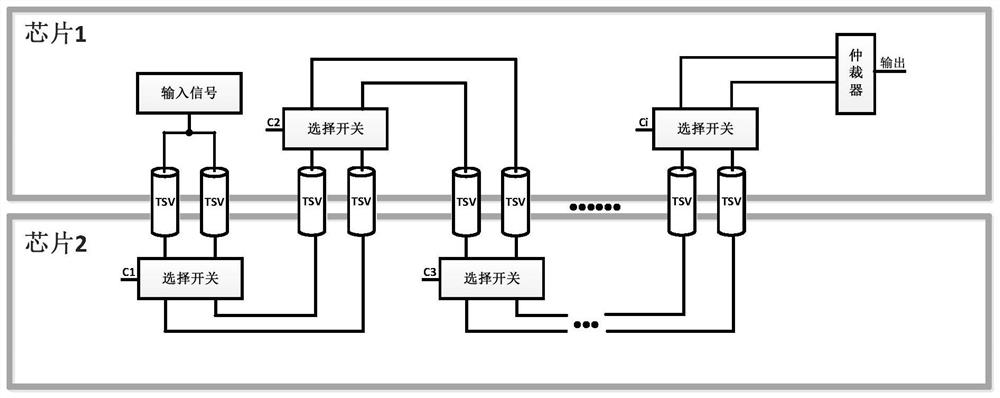
[0034] see figure 1 as well as figure 2 , the present invention provides a security authentication system for 3D stacked chips, including an arbiter PUF circuit and a first chip and a second chip stacked up and down, the first chip and the second chip are associated through a TSV path, and the arbitration The PUF circuit includes two parallel signal paths, the structures of the two signal paths are symmetrical, and path selection switches are arranged at intervals on the signal paths, the TSV paths are connected between the path selection switches, and the two The signal path is connected to the same signal input end, and the output end is connected to the arbiter.

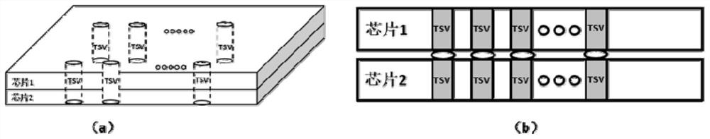
[0035] Such as figure 1 Shown is a schematic diagram of the chip structure based on TSV stacking. Through the manufacture of TSV through holes in the middle of chip 1 and chip 2, the interconnection of chip 1 and chip 2 is realized to achieve the purpose of high speed, low power consumption and miniaturization....

Embodiment 2

[0043] A security authentication method for 3D stacked chips, using the security authentication system for 3D stacked chips in Embodiment 1, such as Image 6 shown, including steps:

[0044] S10. Apply an excitation signal to the arbiter PUF circuit, generate different excitation-response data based on different 3D stacked chips; upload the excitation-response data to the data center;

[0045] S20. Perform stimulus-response verification on the chip before the chip is used, obtain verification data and compare it with the stimulus-response data of the data center, and complete chip security verification.

[0046] Before step S10, a step signal needs to be input at the signal input terminal, which is transmitted simultaneously by the two signal paths; the step signals on the two signal paths respectively enter the path selection switch through the set TSV path.

[0047] Step S10 includes:

[0048] The step signal enters the path selection switch, and the arbiter PUF circuit ap...


PUM


Abstract

The invention provides a security authentication system and method for a 3D stacked chip, and the system comprises an arbiter PUF circuit, a first chip and a second chip, the first chip and the second chip are stacked up and down, the first chip and the second chip are correlated through a TSV path, the arbiter PUF circuit comprises two parallel signal paths, wherein the two signal paths are symmetrical in structure, path selection switches are arranged on the signal paths at intervals, the TSV path is connected between the path selection switches, the two signal paths are connected with the same signal input end, and the output end is connected with an arbiter. The PUF is designed based on the manufacturing deviation of the TSV, different excitation response data are generated by using the RC characteristic of the TSV, and a unique fingerprint of the chip can be formed, so that the chip has an unclonable characteristic, and a security authentication function is provided.

Description

technical field [0001] The invention belongs to the technical field of security authentication, and relates to a security authentication system and method for 3D stacked chips, in particular to a security authentication system and method for 3D stacked chips based on an arbiter PUF circuit. Background technique [0002] At present, as the size of transistors decreases to 5nm, Moore's Law gradually fails. In order to continue Moore's Law, the industry has turned to the direction of 3D stacking. By stacking chips in 3D, the performance of chips can be improved and the area of ​​chips can be reduced. There are many ways to perform 3D stacking of chips, such as stacking by wire-bond or stacking through silicon vias (Through silicon via, TSV). Among them, the chip stacked by TSV first etches the silicon chip to form micro-holes, and then fills copper, tungsten, polysilicon and other conductive substances to realize the vertical electrical interconnection of through-silicon holes...

Claims


Application Information

Patent Timeline
Patent Type & Authority Applications(China)
IPC IPC(8): H04L29/06
CPCH04L63/0876
Inventor 殷中云朱晓锐唐越郑伟坤苏通
Owner SHENZHEN STATE MICROELECTRONICS CO LTD
Features
  • R&D
  • Intellectual Property
  • Life Sciences
  • Materials
  • Tech Scout
  • Unparalleled Data Quality
  • Higher Quality Content
  • 60% Fewer Hallucinations
Learn More