Laminated lead terminal and power module adopting same

A lead terminal and laminated lead technology, applied in the field of power semiconductor devices, can solve problems such as large parasitic inductance, and achieve the effects of reducing parasitic inductance, improving reliability and firm connection

Pending Publication Date: 2021-04-16
华芯威半导体科技(北京)有限责任公司
View PDF0 Cites 0 Cited by
  • Summary
  • Abstract
  • Description
  • Claims
  • Application Information

AI Technical Summary

Problems solved by technology

The parasitic inductance of the traditional packaging structure is large, which can no longer meet the n

Method used


Image

  • Laminated lead terminal and power module adopting same
  • Laminated lead terminal and power module adopting same
  • Laminated lead terminal and power module adopting same

Examples


Example Embodiment

[0030]The technical solutions of the present invention will be described below in conjunction with the drawings, as will be described, as described herein is an embodiment of the invention, not all of the embodiments. Based on the embodiments of the present invention, there are all other embodiments obtained without making creative labor without making creative labor premises.

[0031]In the description of the invention, it is to be described in the terms "center", "upper", "lower", "left", "right", "vertical", "horizontal", "within", "outside", etc. The orientation or positional relationship indicated is based on the orientation or positional relationship shown in the drawings, is merely intended to describe the present invention and simplified description, rather than indicating or implying that the device or component must have a specific orientation. Construct and operation, so it is not understood to be the limitation of the invention. Moreover, the term "first", "second", "third"...


PUM


Abstract

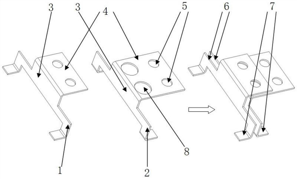
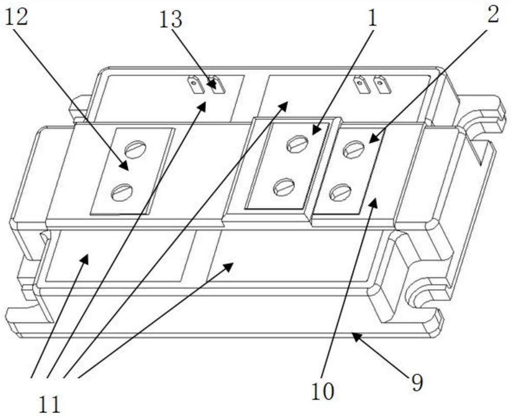
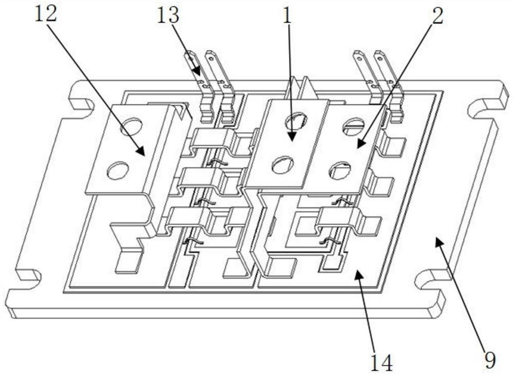
The invention discloses a laminated lead terminal and a power module adopting the same; the laminated lead terminal comprises a first lead terminal and a second lead terminal; the first lead terminal and the second lead terminal each comprise a main body part; one end of the main body part is bent to form a connecting part, and the connecting part is provided with a connecting hole; connecting arms extend from the other end of the main body part towards the two sides and in the direction away from the connecting part, and the tail ends of the connecting arms are bent to form welding feet; the connecting part of the second lead terminal is also provided with a transition hole, the connecting arms of the first lead terminal and the second lead terminal, the main body part and the connecting part are arranged in a laminated manner, and the connecting hole of the first lead terminal is arranged above the transition hole. The lead terminal adopts a laminated structure, so that the parasitic inductance of the power module is reduced, and the oscillation of switching voltage and current waveforms is reduced.

Description

Technical field[0001]The present invention relates to the field of power semiconductor devices, in particular, to a laminated lead terminal and a power module employing the lead terminal.Background technique[0002]The power semiconductor switch chip, such as an IGBT or SiC MOSFET chip, encapsulated inside the power module, thereby achieving high speed switching of large currents. However, since the package structure introduces parasitic inductance, the parasitic inductance causes voltage fluctuations, resulting in voltage overshoot or waveform oscillation, affecting the normal use of the power module. Each power module package manufacturer is trying to reduce parasitic inductance, and end users are also very concerned about this parameter, but there are not many effective methods to reduce parasitic inductance.[0003]In recent years, with the increasingness of the SiC MOSFET device, it is more demanding for parasitic inductance. Only by reducing parasitic inductance can give full play...

Claims


Application Information

Patent Timeline
IPC IPC(8): H01L23/492H01L25/07H01L25/18H01L23/04H01L23/10
CPCH01L2224/40H01L2224/48091H01L2224/73221H01L2924/00014
Inventor 王志超
Owner 华芯威半导体科技(北京)有限责任公司
Why Eureka
Try Eureka