A gallium arsenide solar cell and its preparation method
A technology of solar cells and multi-junction solar cells, applied in the field of solar cells, can solve problems such as limiting the full use of sunlight, reducing solar light transmittance, high absorption, etc., to achieve enhanced current collection capabilities and high solar light transmittance , Improve the effect of high absorption and strong reflection
- Summary
- Abstract
- Description
- Claims
- Application Information
AI Technical Summary
Problems solved by technology
Method used
Image
Examples
preparation example Construction
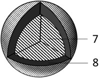
[0041] The present invention is to described TiO 2 The preparation method of @AZO is not particularly limited, and preparation methods well known to those skilled in the art can be used to prepare TiO 2 The method of @AZO core-shell structure, in some specific embodiments provided by the present invention, the TiO used 2 The preparation method of @AZO is: make TiO 2 The particles are suspended in the cavity of the magnetron sputtering machine, and the AZO is evenly sputtered onto the TiO 2 Particle surface, thus obtaining the core-shell structure of TiO 2 @AZO.
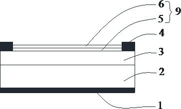
[0042] The present invention uses TiO 2 as the core, AZO as the shell for TiO 2 The preparation of @AZO, and then this TiO 2 @AZO is used as the raw material to make the inner anti-reflection layer 5. Due to the addition of AZO, TiO 2 Has a good conductivity, on the other hand, the core-shell structure of TiO 2 @AZO changed the distribution form of AZO in the inner anti-reflection layer 5, and made it use the ...
Embodiment 1
[0067] 1) A P-type Ge substrate is provided as the substrate layer 2, and a Ge bottom cell, an InGaAs middle cell, a GaInP top cell, and a GaAs contact layer are sequentially grown on the substrate to form a gallium arsenide epitaxial layer 3 to obtain an epitaxial wafer with a substrate.
[0068] 2) Put the epitaxial wafer into the acetone solution and ultrasonically clean it for 10 minutes, then ultrasonically clean it in the isopropanol solution for 10 minutes, and spin-coat the negative photoresist to make the electrode mask pattern.
[0069] 3) Evaporate the metal material Au / AuGeNi / Au / Ag / Au on the upper electrode 4, and use the lift-off stripping process to obtain the upper electrode 4 (the shading rate of the grid line is 3.18%).
[0070] 4) Put the epitaxial wafer into the acetone solution for 10 minutes and ultrasonically clean it for 10 minutes, then ultrasonically clean it in the isopropanol solution for 10 minutes, and vapor-deposit the metal material Pd / Ag / Au of th...
Embodiment 2
[0076] 1) A P-type Ge substrate is provided as the substrate layer 2, and a Ge bottom cell, an InGaAs middle cell, a GaInP top cell, and a GaAs contact layer are sequentially grown on the substrate to form a gallium arsenide epitaxial layer 3 to obtain an epitaxial wafer with a substrate.
[0077] 2) Put the epitaxial wafer into the acetone solution and ultrasonically clean it for 10 minutes, then ultrasonically clean it in the isopropanol solution for 10 minutes, and spin-coat the negative photoresist to make the electrode mask pattern.
[0078] 3) Evaporate the metal material Au / AuGeNi / Au / Ag / Au on the upper electrode 4, and use the lift-off stripping process to obtain the upper electrode 4 (the shading rate of the grid line is 3.18%).
[0079] 4) Put the epitaxial wafer into the acetone solution for 10 minutes and ultrasonically clean it for 10 minutes, then ultrasonically clean it in the isopropanol solution for 10 minutes, and vapor-deposit the metal material Pd / Ag / Au of th...
PUM
| Property | Measurement | Unit |
|---|---|---|
| particle diameter | aaaaa | aaaaa |
| thickness | aaaaa | aaaaa |
| particle diameter | aaaaa | aaaaa |
Abstract
Description
Claims
Application Information

