Automatic chip mounter

An automatic placement machine, wafer technology, applied in electrical components, semiconductor/solid-state device manufacturing, circuits, etc., can solve problems affecting the mounting accuracy of wafers and substrates

Active Publication Date: 2021-04-23
微见智能封装技术(深圳)有限公司
View PDF5 Cites 2 Cited by
  • Summary
  • Abstract
  • Description
  • Claims
  • Application Information

AI Technical Summary

Problems solved by technology

[0004] In order to solve the problem of misalignment between the wafer and the substrate due to weak contact, which affe

Method used


Image

  • Automatic chip mounter
  • Automatic chip mounter
  • Automatic chip mounter

Examples


Embodiment Construction

[0034] In order to make the purpose, technical solutions and advantages of the present invention more clear, the present invention will be further described in detail below in conjunction with the accompanying drawings and implementation examples. It should be understood that the specific embodiments described here are only used to explain the present invention, not to limit the present invention.

[0035] It should be noted that when an element is referred to as being “fixed” to another element, it can be directly on the other element or there can also be an intervening element. When an element is referred to as being "connected to" another element, it can be directly connected to the other element or intervening elements may also be present. The terms "vertical," "horizontal," "left," "right," and similar expressions are used herein for purposes of illustration only.

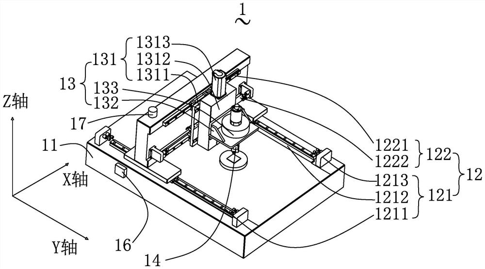
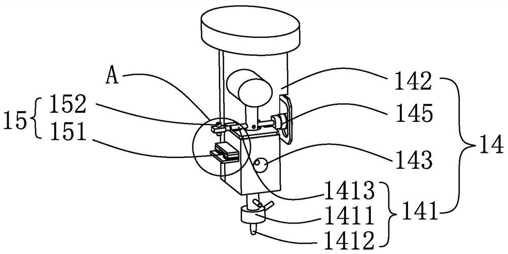
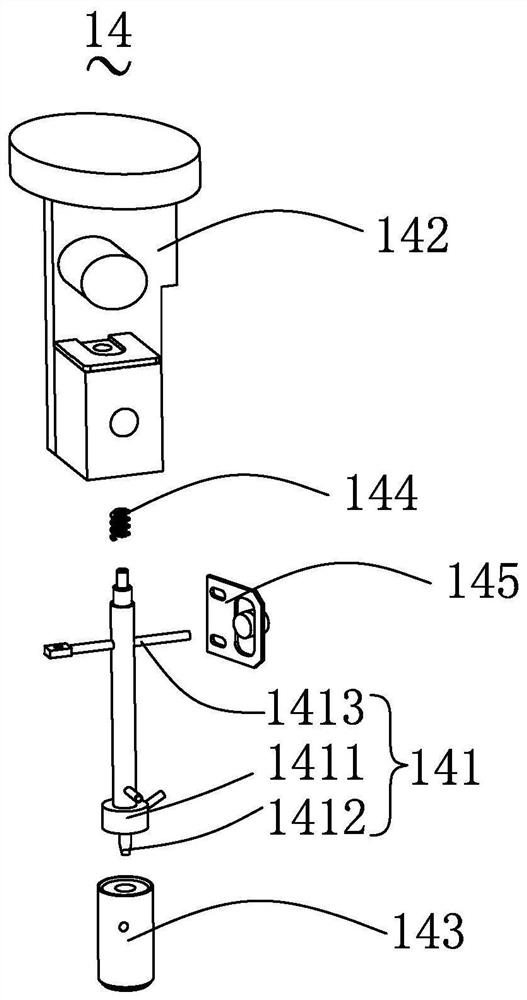
[0036] see figure 1 and figure 2 , the first embodiment of the present invention provides an automatic ch...


PUM

PropertyMeasurementUnit
Thicknessaaaaaaaaaa

Abstract

The invention relates to the technical field of chip mounters, in particular to an automatic chip mounter. The automatic chip mounter comprises a driving assembly, a die bonding assembly and a sensing assembly which are connected in sequence. The die bonding assembly is used for sucking a wafer, the driving assembly drives the die bonding assembly to place the wafer on a substrate for bonding, and the sensing assembly detects the pressure between the wafer and the substrate when the wafer is bonded by the die bonding assembly. According to the design, the pressure when the wafer is attached to the substrate is detected, so that the phenomenon that the wafer and the substrate are not firmly attached or misplaced due to the fact that the attaching pressure between the wafer and the substrate is too small when an automatic chip mounter is used for die bonding can be avoided, meanwhile, the wafer can be prevented from being damaged due to the fact that the attaching pressure between the wafer and the substrate is too large, and by detecting the pressure when the wafer is attached to the substrate, the mounting precision between the wafer and the substrate during die bonding by the automatic chip mounter is further improved.

Description

【Technical field】 [0001] The invention relates to the technical field of placement machines, in particular to an automatic placement machine. 【Background technique】 [0002] In the packaging process of electronic equipment, die bonding is one of the most important links. In the early days, mechanical die bonding equipment was usually used to install the chip on the substrate. The placement machine can realize fully automatic and high-speed solid crystal on the substrate; [0003] The commonly used high-speed automatic chip mounter is to pick up and place the chip through the vacuum nozzle. When the vacuum nozzle places the chip on the corresponding position of the substrate, the chip only contacts the substrate by its own gravity, which leads to the chip Due to the weak contact with the substrate, dislocation is prone to occur, which in turn affects the mounting accuracy between the chip and the substrate. At the same time, the above-mentioned automatic placement machine ca...

Claims


Application Information

Patent Timeline
IPC IPC(8): H01L21/67H01L21/68H01L21/683
CPCH01L21/67121H01L21/6838H01L21/68
Inventor 雷伟庄
Owner 微见智能封装技术(深圳)有限公司
Why Eureka
Try Eureka