Multi-layer stacked packaging structure and preparation method of multi-layer stacked packaging structure
A packaging structure and multi-layer stacking technology, applied in semiconductor/solid-state device manufacturing, electrical components, electric solid-state devices, etc. Limitation and other issues, to achieve the effect of heat dissipation and wire bonding, increase the number of stacks, and reduce the size of the package
- Summary
- Abstract
- Description
- Claims
- Application Information
AI Technical Summary
Problems solved by technology
Method used
Image

Examples
no. 1 example
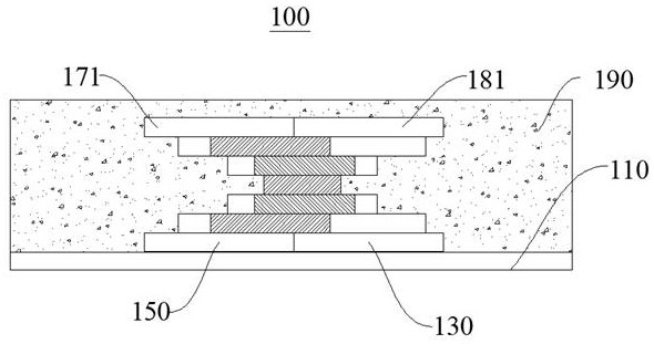
[0048] see in conjunction Figure 1 to Figure 7 , this embodiment provides a multi-layer stacked packaging structure 100, which adopts a bidirectional spiral stacking method, which can increase the number of stacks, reduce the size of the stack, ensure the stability of the structure, and increase the integration of the product.
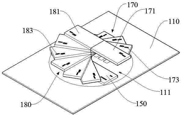
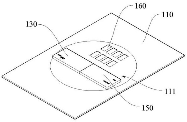
[0049] The multilayer stack package structure 100 provided in this embodiment includes a substrate 110, a first base chip 130, a second base chip 150, a plurality of first structure chips 171, a plurality of second structure chips 181 and a plastic package 190, the first The base chip 130 and the second base chip 150 are mounted on the substrate 110, and the first base chip 130 and the second base chip 150 are centrally symmetrically arranged, and the first base chip 130 and the second base chip 150 are electrically connected to the substrate 110 . A plurality of first structure chips 171 are mounted on the first base chip 130, and the plurality of f...
no. 2 example
[0068] see Figure 8 , a multi-layer stack package structure 100 provided in this embodiment, its basic structure, principle and technical effects are the same as those of the first embodiment. Corresponding content in the embodiment.
[0069] In this embodiment, the multilayer stack package structure 100 includes a substrate 110, a first base chip 130, a second base chip 150, a plurality of first structure chips 171, a plurality of second structure chips 181 and a plastic package 190, the first The base chip 130 and the second base chip 150 are mounted on the substrate 110, and the first base chip 130 and the second base chip 150 are centrally symmetrically arranged, and the first base chip 130 and the second base chip 150 are electrically connected to the substrate 110 . A plurality of first structure chips 171 are mounted on the first base chip 130, and the plurality of first structure chips 171 are spirally stacked on the first base chip 130, and form an electrical conne...
no. 3 example
[0076] This embodiment provides a multi-layer stack package structure 100. Its basic structure, principle and technical effect are the same as those of the first embodiment. For a brief description, the part not mentioned in this embodiment can refer to the first embodiment corresponding content in the example.
[0077] The multilayer stack package structure 100 provided in this embodiment includes a substrate 110, a first base chip 130, a second base chip 150, a plurality of first structure chips 171, a plurality of second structure chips 181, and a plastic package 190. The first base The chip 130 and the second base chip 150 are mounted on the substrate 110 , and the first base chip 130 and the second base chip 150 are arranged symmetrically to the center, and the first base chip 130 and the second base chip 150 are electrically connected to the substrate 110 . A plurality of first structure chips 171 are mounted on the first base chip 130, and the plurality of first structu...
PUM
 Abstract
Description
Claims
Application Information
 - R&D
- Intellectual Property
- Life Sciences
- Materials
- Tech Scout
- Unparalleled Data Quality
- Higher Quality Content
- 60% Fewer Hallucinations
Browse by: Latest US Patents, China's latest patents, Technical Efficacy Thesaurus, Application Domain, Technology Topic, Popular Technical Reports.
© 2025 PatSnap. All rights reserved.Legal|Privacy policy|Modern Slavery Act Transparency Statement|Sitemap|About US| Contact US: help@patsnap.com