Micro OLED display structure and preparation method thereof
A display structure, ring-shaped technology, applied in semiconductor/solid-state device manufacturing, semiconductor devices, electrical components, etc., can solve problems such as reducing packaging reliability, improve reliability, reduce the risk of piercing the multi-layer structure, improve quality effect
- Summary
- Abstract
- Description
- Claims
- Application Information
AI Technical Summary
Problems solved by technology
Method used
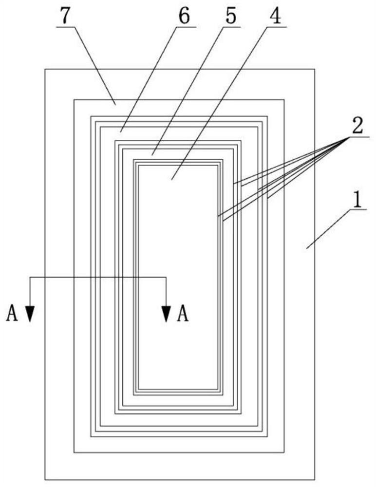
Image


Examples
Embodiment Construction
[0027] In order to make the purpose, technical solutions and advantages of the embodiments of the present invention more clear, the technical solutions in the embodiments will be clearly and completely described below in conjunction with the drawings in the embodiments of the present invention. The following embodiments are used to illustrate the present invention , but not to limit the scope of the present invention.
[0028] In the description of the present invention, it should be noted that the terms "upper", "lower", "front", "rear", "left", "right", "vertical", "inner", "outer" etc. The indicated orientation or positional relationship is based on the orientation or positional relationship shown in the drawings, and is only for the convenience of describing the present invention and simplifying the description, rather than indicating or implying that the referred device or element must have a specific orientation, or in a specific orientation. construction and operation, ...
PUM
| Property | Measurement | Unit |
|---|---|---|
| Top width | aaaaa | aaaaa |
| Bottom width | aaaaa | aaaaa |
Abstract
Description
Claims
Application Information
 - R&D
- Intellectual Property
- Life Sciences
- Materials
- Tech Scout
- Unparalleled Data Quality
- Higher Quality Content
- 60% Fewer Hallucinations
Browse by: Latest US Patents, China's latest patents, Technical Efficacy Thesaurus, Application Domain, Technology Topic, Popular Technical Reports.
© 2025 PatSnap. All rights reserved.Legal|Privacy policy|Modern Slavery Act Transparency Statement|Sitemap|About US| Contact US: help@patsnap.com