
An automatic smearing device for silicon wafer coating and its application method

A technology of driving device and silicon wafer, which is applied to the device and coating of the surface coating liquid, which can solve the problems of low efficiency, poor continuity, and environmental deterioration of the processing workshop, so as to avoid glue exposure, protect the environment, and protect the environment. Increase the effect of the spray effect

Active Publication Date: 2022-04-19
无锡优联创芯机电设备有限公司
View PDF6 Cites 0 Cited by
  • Summary
  • Abstract
  • Description
  • Claims
  • Application Information

AI Technical Summary

Problems solved by technology

[0003] The existing device has poor continuity when applying glue to silicon wafers, and requires manual participation, so the efficiency is not high. In addition, when applying glue, mechanized operations can easily cause uneven application of silicon wafers, and the exposed glue will cause the environment of the processing workshop to deteriorate.

Method used


Image

  • An automatic smearing device for silicon wafer coating and its application method
  • An automatic smearing device for silicon wafer coating and its application method
  • An automatic smearing device for silicon wafer coating and its application method

Examples


Embodiment Construction

[0029] The following will clearly and completely describe the technical solutions in the embodiments of the present invention with reference to the accompanying drawings in the embodiments of the present invention. Obviously, the described embodiments are only some, not all, embodiments of the present invention. Based on the embodiments of the present invention, all other embodiments obtained by persons of ordinary skill in the art without making creative efforts belong to the protection scope of the present invention.

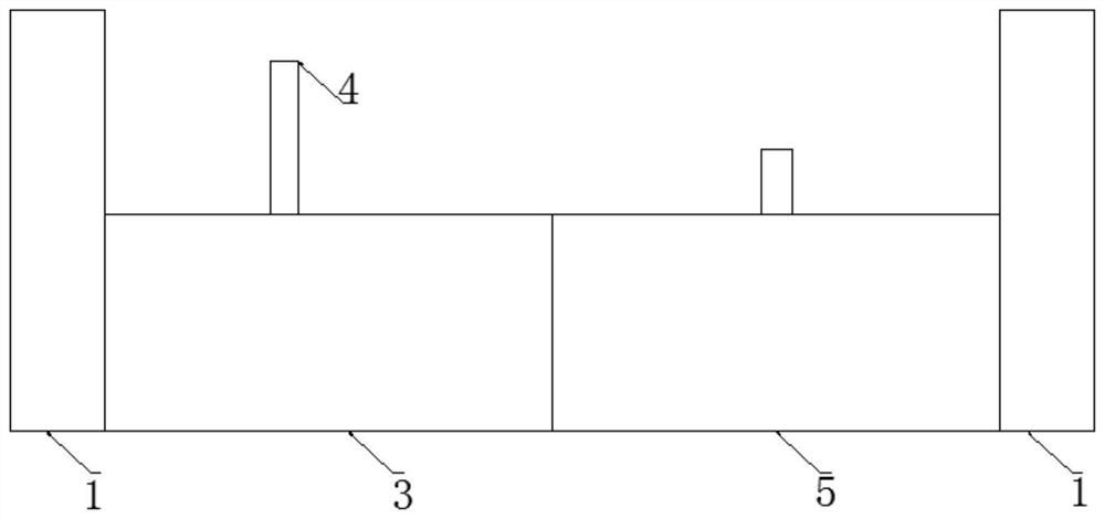
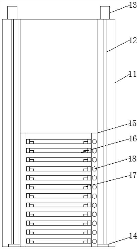
[0030] Such as Figure 1-6 As shown, the present invention provides a technical solution: an automatic silicon wafer smearing device, comprising two elevating devices 1, the right side of the elevating device 1 on the left is fixedly connected with a wafer gluing drive device 3, the wafer The right side of the gluing driving device 3 is fixedly connected with a drying device 5, and the right side of the drying device 5 is fixedly connected with the lifting dev...


PUM


Abstract

The invention relates to the technical field of an automatic silicon wafer smearing device, and discloses a method for using an automatic silicon wafer smearing device, which includes two lifting devices, and the right side of the lifting device on the left side is fixedly connected There is a wafer gluing driving device, a drying device is fixedly connected to the right side of the wafer gluing driving device, and the right side of the drying device is fixedly connected to the lifting device on the right side. The present invention improves the transmission device. During transmission, the fourth forward and reverse motor drives the third screw to rotate, and the third screw moves the mounting strips on the two third ball sleeves to the opposite side. In this way, When the installation bar moves to the appropriate position, the third forward and reverse motor starts, and the two transmission wheels drive the transmission belt to rotate. When the silicon wafer falls on the two transmission belts, it can be transmitted. When it reaches the designated position, the first The four forward and reverse motors are started, so that the two third ball sleeves move towards opposite directions, and at this time, the silicon wafer can be put down.

Description

technical field [0001] The invention relates to the technical field of a coating device for automatic silicon wafer coating, in particular to an automatic coating device for coating coating of silicon wafers and a use method. Background technique [0002] With the development of production and technology in the semiconductor industry, the automation requirements for production equipment are getting higher and higher. Gluing treatment of silicon wafers is an essential link in the semiconductor industry. In the past, the gluing of silicon wafers was mostly done manually, the work efficiency was low, and it was difficult to guarantee the final film thickness and uniformity. In recent years, with the continuous research of technicians, automatic gluing machines have been widely used in the semiconductor industry. At present, the equipment process generally used in the gluing treatment of silicon wafers in the semiconductor industry is to manually place the basket and automatica...

Claims


Application Information

Patent Timeline
Patent Type & Authority Patents(China)
IPC IPC(8): B05C5/02B05C13/02B05C15/00
CPCB05C5/0208B05C13/02B05C15/00
Inventor 谢辉平
Owner 无锡优联创芯机电设备有限公司
Learn More