Display device and preparation method thereof

A technology for display devices and metal layers, applied in identification devices, semiconductor/solid-state device manufacturing, instruments, etc., can solve problems such as poor bending resistance, too wide connecting bridge area, fracture failure, etc., to reduce the risk of fracture failure , Improve the bending resistance and reduce the overall width

Pending Publication Date: 2021-05-14
WUHAN CHINA STAR OPTOELECTRONICS SEMICON DISPLAY TECH CO LTD
View PDF0 Cites 0 Cited by
  • Summary
  • Abstract
  • Description
  • Claims
  • Application Information

AI Technical Summary

Problems solved by technology

At present, the metal layer in the pixel island area is often made of titanium, molybdenum, and titanium layered composite structure (Ti / Mo / Ti) to make the gate, source, drain, and gate wiring, source wiring, and drain wiring. Because the metal layer containing molybdenum has poor bending resistance, this metal layer is not suitable for making metal traces in the connection bridge area
At the same time, parallel wiring on the same layer is usually used in the connection bridge area, and a certain distance is reserved in the horizontal direction to prevent short circuits, which will cause the connection bridge area to be too wide and affect the bending performance of the connection bridge area.
[0005] To sum up, in the prior art, there are technical problems that the width of the connecting bridge area of ​​the display device is too large, the bending resistance is poor, and the fracture and failure are prone to occur during the stretching process, which further affects the normal display of the display device.

Method used


Image

  • Display device and preparation method thereof
  • Display device and preparation method thereof
  • Display device and preparation method thereof

Examples


Embodiment Construction

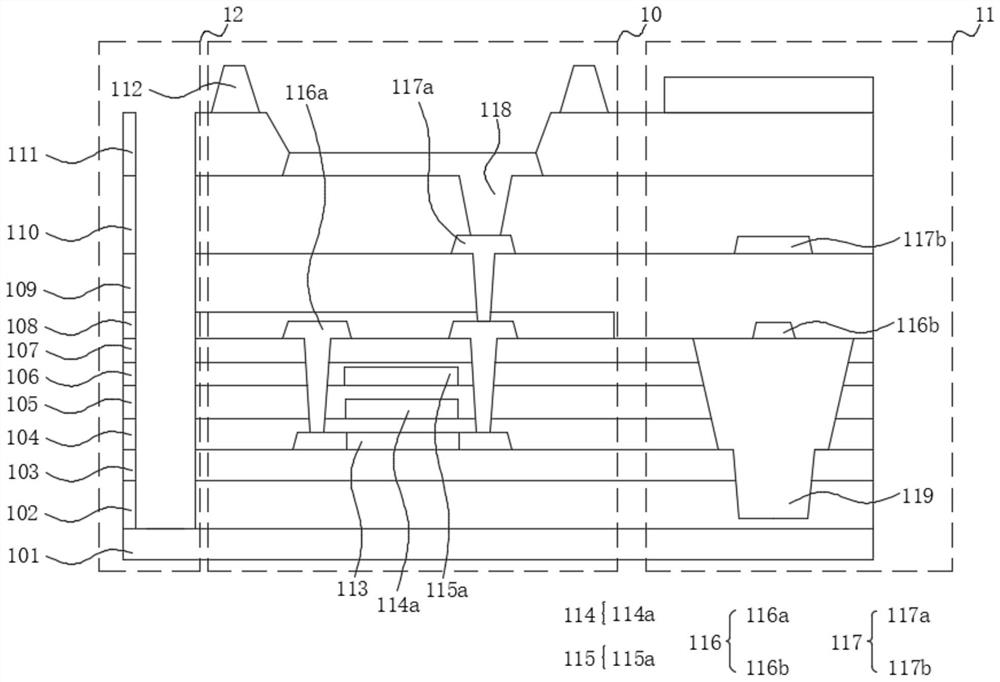
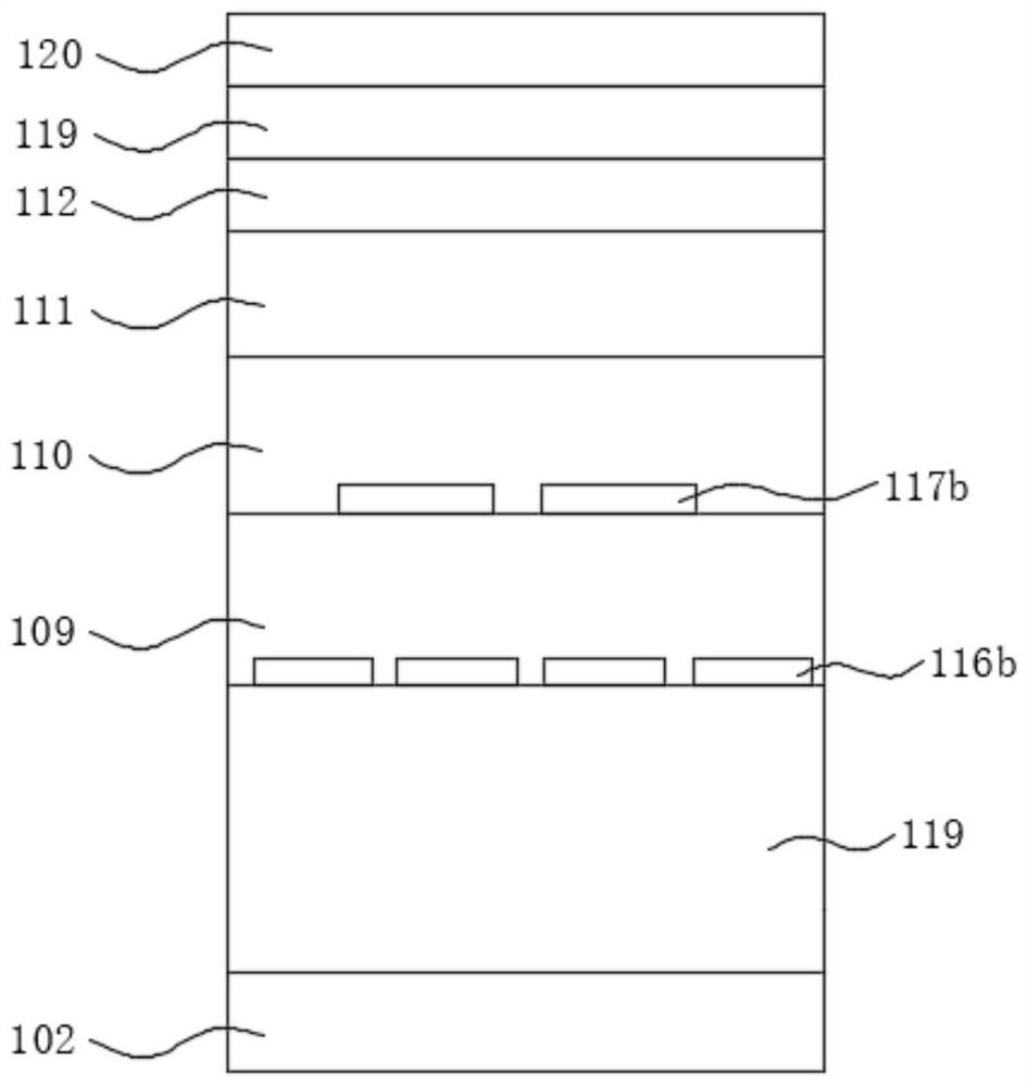
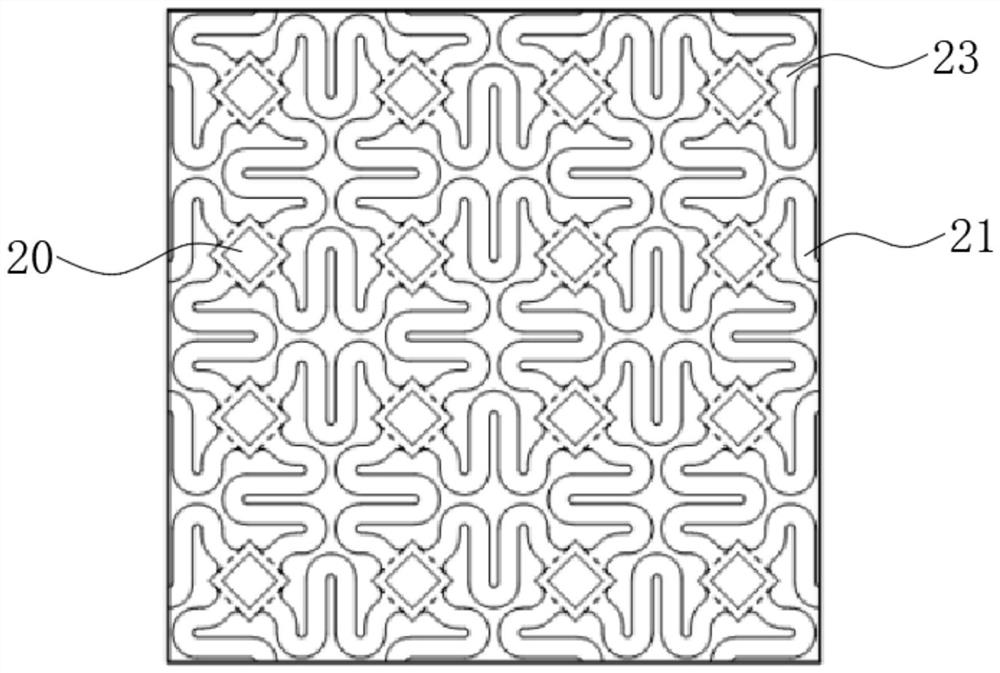
[0037] The following will clearly and completely describe the technical solutions in the embodiments of the present invention with reference to the drawings in the embodiments of the present invention. Apparently, the described embodiments are only some of the embodiments of the present invention, but not all of them. Based on the embodiments of the present invention, all other embodiments obtained by those skilled in the art without creative efforts fall within the protection scope of the present invention.

[0038] In describing the present invention, it is to be understood that the terms "center", "length", "width", "thickness", "upper", "lower", "left", "right", "vertical", The orientation or positional relationship indicated by "horizontal", etc. is based on the orientation or positional relationship shown in the drawings, and is only for the convenience of describing the present invention and simplifying the description, rather than indicating or implying that the referr...


PUM


Abstract

The invention discloses a display device and a preparation method thereof. The display device comprises: a plurality of pixel island regions which are separated from one another; and a plurality of connection bridge regions, wherein the adjacent pixel island regions are connected with each other through the plurality of connection bridge regions. The display device comprises a first metal layer, the first metal layer is patterned in the pixel island area to form an anode, and the first metal layer is patterned in the connecting bridge area to form at least one metal wire. The metal wires are formed in the connecting bridge area through the first metal layer, the number of film layers forming the metal wires is increased, the number of the film layers in the same film layer is reduced and the overall width of the connecting bridge area is reduced under the condition that the number of photomasks and the manufacturing process number of the photomasks are not increased, so that the bending resistance is improved, the risk of fracture failure in the stretching process is reduced, and the product quality is improved.

Description

technical field [0001] The invention relates to the field of display technology, in particular to a display device and a method for preparing the display device. Background technique [0002] Compared with foldable and rollable display screens, stretchable flexible display screens have the characteristics of thinness, low power consumption, and adjustable mechanical properties. The screen can be stretched in any direction and still ensure a good display effect. It is the next generation One of the key directions of new flexible display research. [0003] In the current display device, in order to facilitate the tensile strain, the flexible polyimide (Polyimide, PI) substrate is scattered in the shape of islands, and these polyimide islands are connected by ribbon-shaped connecting bridge (Hinge) regions. The pixel circuits are distributed on the polyimide islands, and the metal traces between the pixel circuits are distributed on the strip connection bridge area. [0004] ...

Claims


Application Information

Patent Timeline
IPC IPC(8): H01L27/12H01L21/84G09F9/30
CPCH01L27/1218H01L27/1244H01L27/1288H01L27/1262G09F9/301Y02E10/549H10K59/122H10K59/131H10K59/35
Inventor 程立昆孙亮易士娟
Owner WUHAN CHINA STAR OPTOELECTRONICS SEMICON DISPLAY TECH CO LTD
Why Eureka
Try Eureka