Resonating device and filter

A device and resonance technology, applied in the field of resonant devices and filters, can solve the problems of increasing the manufacturing cost of BAW resonant devices, high cost, and the inability to take into account device power threshold, insertion loss and manufacturing cost at the same time

Pending Publication Date: 2021-05-14
SPECTRON (SHENZHEN) TECH CO LTD
View PDF0 Cites 1 Cited by
  • Summary
  • Abstract
  • Description
  • Claims
  • Application Information

AI Technical Summary

Problems solved by technology

At present, in order to meet the needs of mobile broadband and high data rate wireless applications, modern communication standards continue to develop towards higher frequencies and wider bandwidths. The SAW resonant devices and BAW resonant devices in the prior art can no longer meet the above standards
[0004] For example, the SAW resonant device has the advantage of low cost, but the operating frequency of the SAW resonant device is low. To increase the operating frequency of the SAW resonant device, the electrode width of the resonant device needs to be adjusted, so that the design of the SAW resonant device cannot take into account the power threshold, insertion loss, and manufacturing cost, resulting in high-frequency SAW resonators that are either cost prohibitive or perform poorly
Although BAW resonant devices have advantages in performance and high frequency, the manufacturing process of BAW resonant devices is complicated, which increases the manufacturing cost of BAW resonant devices and is difficult to meet the needs of the consumer electronics market.

Method used


Image

  • Resonating device and filter
  • Resonating device and filter
  • Resonating device and filter

Examples


Embodiment Construction

[0049]The present invention is further detailed in conjunction with the accompanying drawings and examples. It will be appreciated that the specific embodiments described herein are merely illustrative of the invention and are not limited thereto. It will also be noted that in order to facilitate the description, only the parts associated with the present invention are shown in the drawings rather than all structures.

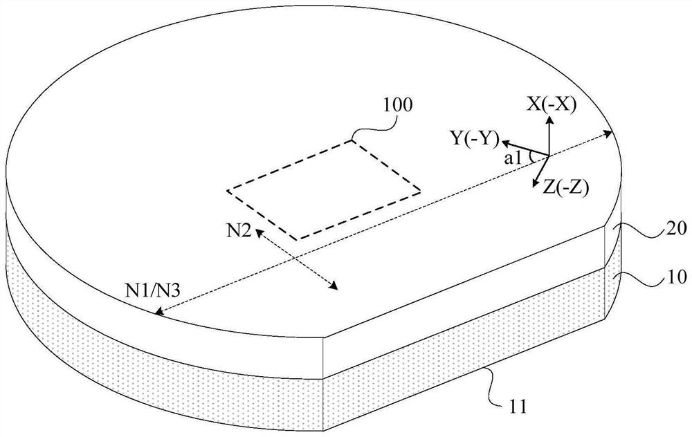
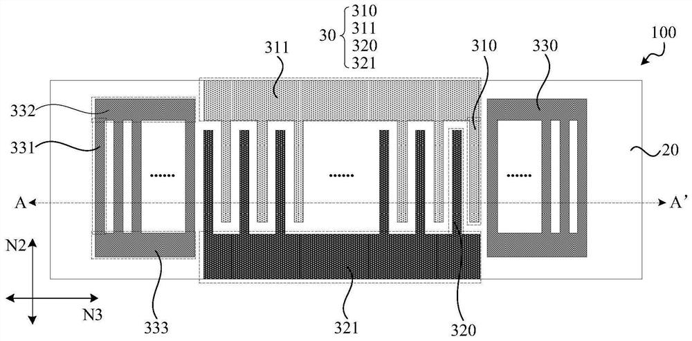
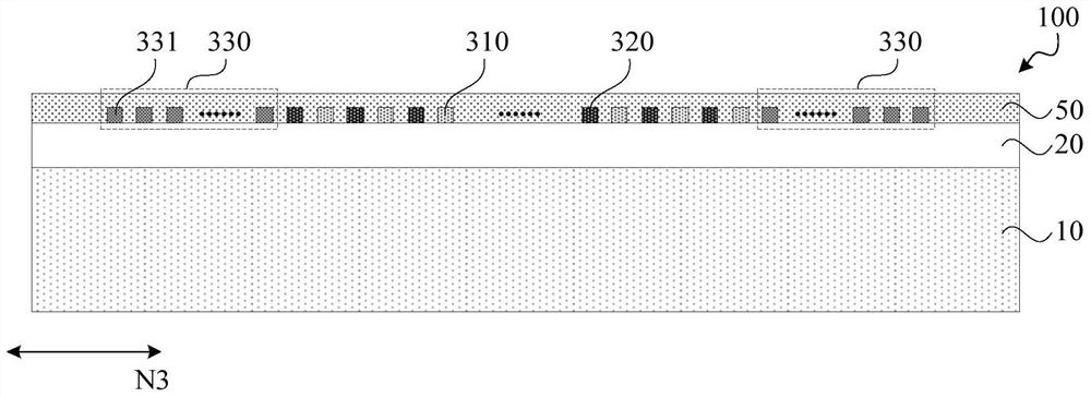
[0050]Embodiments of the present invention provide a resonant device,figure 1 It is a structural diagram of a resonant device according to an embodiment of the present invention, specifically a side view of a wafer-level resonant device, whereinfigure 1 The wafer substrate 10 and the piezoelectric layer 20 of the wafer stage resonant device may only be shown to include a plurality of resonant devices, and the wafer-level resonant device.figure 1 One resonant device 100 is shown;figure 2 It is a top view of a resonant device according to an embodiment of the present inve...


PUM

PropertyMeasurementUnit
Resonant frequencyaaaaaaaaaa
electromechanical coupling coefficientaaaaaaaaaa

Abstract

The embodiment of the invention discloses a resonance device and a filter. The resonance device comprises a wafer substrate, a piezoelectric layer and an interdigital electrode layer. The piezoelectric layer comprises a piezoelectric single crystal material; the main positioning edge of the wafer substrate is located in a first direction, and the piezoelectric single crystal material comprises a first crystal axis, a second crystal axis and a third crystal axis; the first crystal axis is perpendicular to the wafer substrate, or the first crystal axis is parallel to the wafer substrate, and the included angle between the first crystal axis and the first direction is smaller than or equal to 30 degrees, or larger than or equal to 60 degrees and smaller than or equal to 120 degrees; and the second crystal axis is parallel to the wafer substrate, and the included angle between the second crystal axis and the first direction is smaller than or equal to 60 degrees, or the included angle between the second crystal axis and the direction perpendicular to the wafer substrate is larger than or equal to 120 degrees and smaller than or equal to 135 degrees. According to the technical scheme, the advantage of low cost of the resonator device is guaranteed, the performance and the working frequency of the resonator device are improved, the performance of the band-pass filter comprising the resonator device is improved, and the requirement of the 5G communication standard is met.

Description

Technical field[0001]Embodiments of the present invention relate to wireless communication technology, and more particularly to a resonant device and a filter.Background technique[0002]The radio frequency filter device is an important part of the front end of the wireless communication, with a frequency selection and the function of suppressing the interference signal. A well-performance RF filter device can not only improve the sensitivity of the transmitter, reduce the spectrum occupancy space of the transmitter, but also improve the signal noise ratio of the transceiver, and reduce the power consumption of mobile devices in the communication link.[0003]The radio frequency filtering device consists of a resonant device, and the resonant device typically includes a SURFCE Acoustic Wave, a Bulk Acoustic Wave (BAW) resonator, the SAW resonant device, and the BAW resonator have different frequencies. Technology and cost advantages. Currently, in order to meet the needs of mobile broad...

Claims


Application Information

Patent Timeline
Patent Type & Authority Applications(China)
IPC IPC(8): H03H9/17H03H3/02H03H9/54
CPCH03H3/02H03H9/17H03H9/54H03H2003/027
Inventor 龚颂斌杨岩松
Owner SPECTRON (SHENZHEN) TECH CO LTD
Why Eureka
Try Eureka