

Bulk acoustic wave resonator and semiconductor device
A bulk acoustic wave resonator and cavity technology, applied in electrical components, impedance networks, etc., can solve problems such as performance parameter decline, and achieve the effect of improving the acoustic impedance ratio, reducing loss, and making up for the reduction of Qsw.
- Summary
- Abstract
- Description
- Claims
- Application Information
AI Technical Summary
Problems solved by technology
Method used
Image

Examples
Embodiment Construction
[0043] In order to make the technical problems, technical solutions and beneficial effects to be solved by the present invention clearer, the present invention will be further described in detail below in conjunction with the accompanying drawings and embodiments. It should be understood that the specific embodiments described here are only used to explain the present invention, not to limit the present invention.
[0044] The present invention will be further described in detail below in conjunction with the accompanying drawings and specific embodiments.
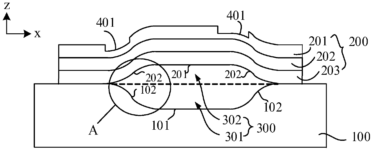
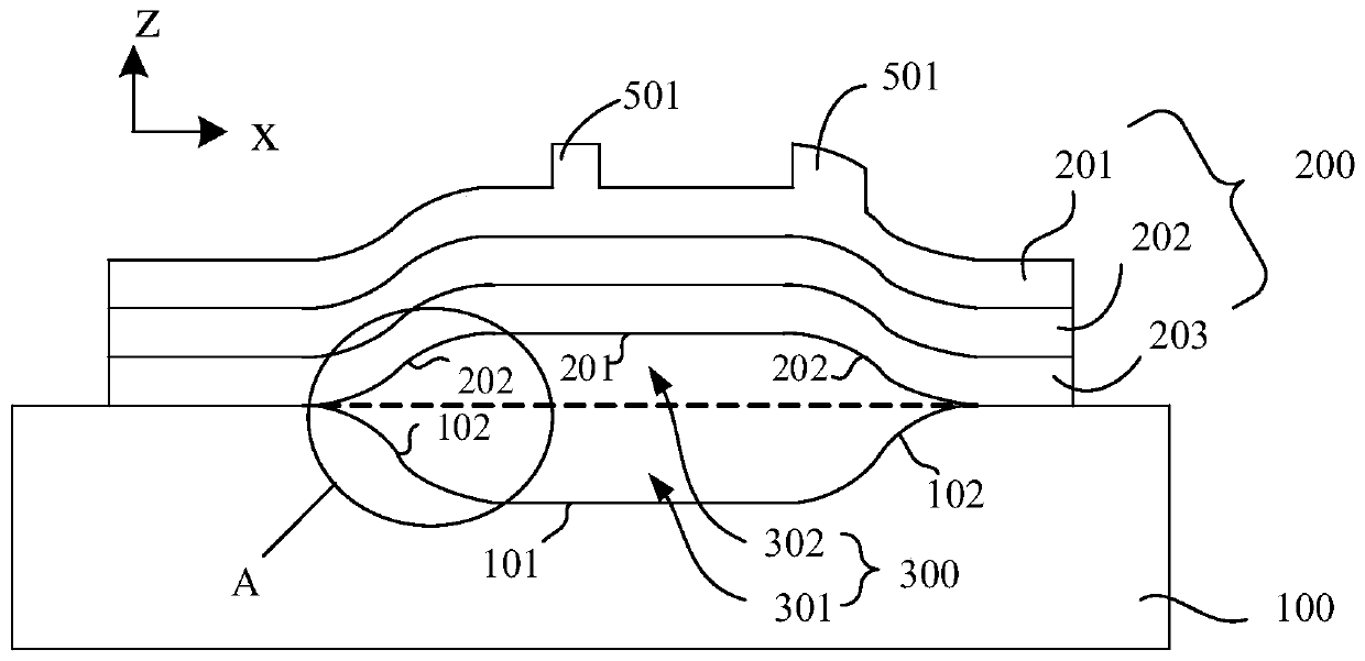
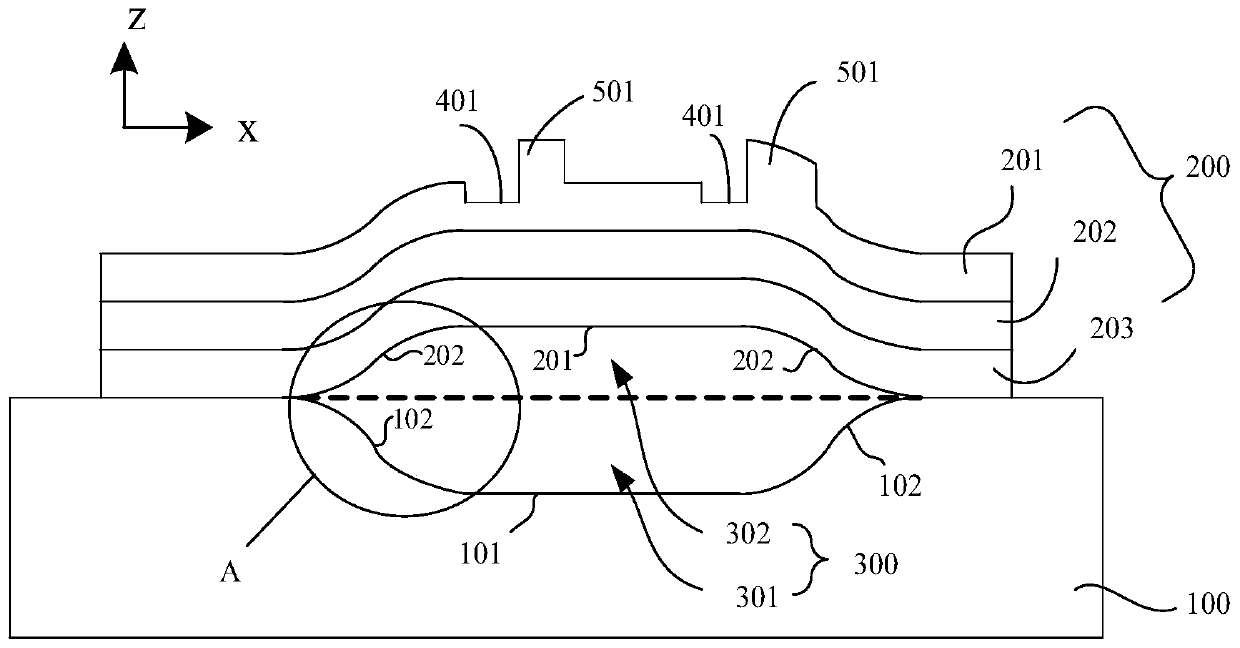
[0045] An embodiment of the present invention provides a bulk acoustic wave resonator, and the bulk acoustic wave resonator includes: a substrate and a multilayer structure. Wherein, a multilayer structure is formed on the substrate, and the multilayer structure includes a lower electrode layer, a doped piezoelectric layer and an upper electrode layer sequentially from bottom to top. A cavity is formed between the substra...
PUM
| Property | Measurement | Unit |
|---|---|---|
| width | aaaaa | aaaaa |
| thickness | aaaaa | aaaaa |
Abstract
Description
Claims
Application Information