
Tunable directional generation on-chip diffraction-free beam device and implementation method thereof

A technology of non-diffraction beams and implementation methods, applied in the field of on-chip devices, can solve problems such as unadjustable and controllable, strong background interference, and insufficient degrees of freedom

Inactive Publication Date: 2021-05-18
GUILIN UNIV OF ELECTRONIC TECH
View PDF2 Cites 1 Cited by
  • Summary
  • Abstract
  • Description
  • Claims
  • Application Information

AI Technical Summary

Problems solved by technology

It has been reported that by fabricating ridge structures on metal films, SPPs beams can become zero-order or first-order Bessel beams, and the zero-order Bessel SPPs beams can reduce the diffraction effect when passing through cylindrical obstacles [Optics Letters, 2013, 38, 905-907], but the non-diffraction SPPs beam produced by this structure has a unique propagation direction, which cannot be adjusted and controlled
Although some studies have reported that the generation of zero-order Bessel-like non-diffraction-like SPPs beams can be controlled in two directions this year, the degree of freedom of regulation is still insufficient, and it is very regrettable that when the zero-order Bessel-like non-diffraction SPPs When the beam is launched in a certain direction, it will generate a first-order Bessel-like SPPs beam in the opposite direction, which will bring strong background interference [Nanomaterials, 2018, 8, 975]

Method used


Image

  • Tunable directional generation on-chip diffraction-free beam device and implementation method thereof
  • Tunable directional generation on-chip diffraction-free beam device and implementation method thereof
  • Tunable directional generation on-chip diffraction-free beam device and implementation method thereof

Examples


Embodiment Construction

[0026] The present invention will be specifically described below by taking a device for generating multiple non-diffracting beams on a chip with tunable orientation and its implementation method as an example.

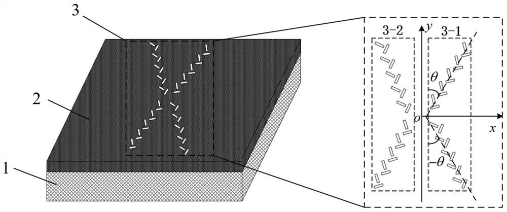
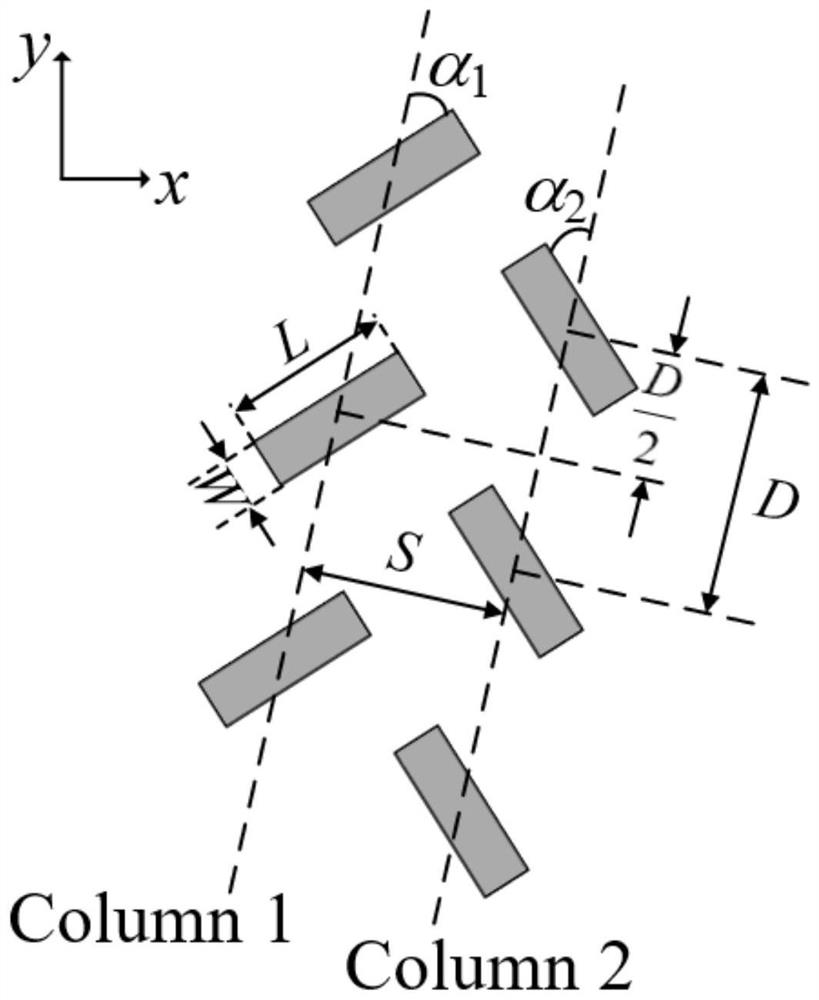
[0027] Such as figure 1 As shown, in this embodiment, the device capable of generating multiple on-chip non-diffracting beams with tunable orientation includes a silicon dioxide substrate 1, a nano-gold film 2, and nanostructure arrays 3-1, 3-2. The basic structures of the nanostructure arrays 3-1 and 3-2 are a pair of rectangular nanoslots. The width of a single rectangular nano-groove is 40nm, the length is 200nm, and its rotation angle is 45 degrees or -45 degrees, etched on the nano-gold film 2 with a height of 200nm, and the nano-gold film 2 is located on the silicon dioxide substrate , the lateral distance between the same pair of rectangular nanoslots is λ spp / 4, the longitudinal distance is 150nm, the structure is as figure 2 shown. For left-handed circu...


PUM

PropertyMeasurementUnit
widthaaaaaaaaaa
lengthaaaaaaaaaa
heightaaaaaaaaaa

Abstract

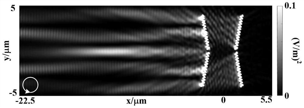
The invention provides a tunable directional generation on-chip non-diffraction beam device and an implementation method thereof. The device structure is characterized by comprising a substrate 1, a nano metal film 2 and a nano structure array 3, the nano-structure array 3 comprises two sub-arrays 3-1 and 3-2 which have different responses to different incident light polarization states, so that the responses of the different polarization states have spatial discrimination, and the nano-structure array 3 has a function similar to a space lens. The specific implementation method comprises the steps that the nano structure array 3 is obtained on the surface of a nanometal film 2 in a focused ion beam etching mode, specific polarization state incident light is input from the lower surface of the substrate 1, an input signal forms a surface plasmon polariton (SPPs) light field on the surface of the nano metal film 2, and due to the special arrangement mode of the nano structure array 3, the generated SPPs light field is focused to form a non-diffraction light beam, and the polarization state and the incident angle of the incident light are changed so as to adjust the emission direction of the non-diffraction light beam.

Description

[0001] (1) Technical field [0002] The invention relates to the fields of all-optical calculation and all-optical information processing, and is especially suitable for manufacturing on-chip devices that generate special light fields. [0003] (2) Background technology [0004] Due to the long response time and high heat loss of electronic components in traditional communication systems, the communication speed of communication systems using traditional electrical components has reached a bottleneck and has a large energy loss. On-chip optical devices are an effective way to solve these problems, so all-optical communication is considered to be the next generation of information processing technology. Among them, the generation and transmission of on-chip optical signals is one of the core technologies of all-optical communication. How to effectively generate on-chip optical signals and ensure that they can be received and processed by the next-level equipment has become a fro...

Claims


Application Information

Patent Timeline
Patent Type & Authority Applications(China)
IPC IPC(8): G02B5/00
CPCG02B5/008
Inventor 刘厚权权志强苑立波
Owner GUILIN UNIV OF ELECTRONIC TECH
Learn More