Transfer device, transfer system and transfer method

A transfer device and transfer substrate technology, which can be used in the manufacture of electrical components, electrical solid-state devices, semiconductor/solid-state devices, etc., and can solve problems such as difficulty in supporting MicroLEDs

Pending Publication Date: 2021-05-18
NANCHANG GUANGHENG ELECTRONIC CENT (LP)
View PDF0 Cites 1 Cited by
  • Summary
  • Abstract
  • Description
  • Claims
  • Application Information

AI Technical Summary

Problems solved by technology

Due to the problems of transfer efficiency, yield and precision, it is difficult to

Method used


Image

  • Transfer device, transfer system and transfer method
  • Transfer device, transfer system and transfer method
  • Transfer device, transfer system and transfer method

Examples


Embodiment Construction

[0045] The present invention will be further described in detail below in conjunction with the accompanying drawings and embodiments. It should be understood that the specific embodiments described here are only used to explain the present invention, but not to limit the present invention. In addition, it should be noted that, for the convenience of description, only some structures related to the present invention are shown in the drawings but not all structures.

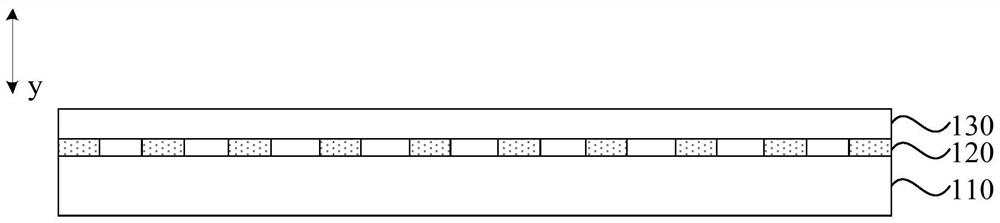
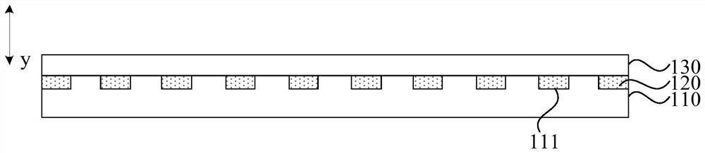
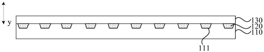
[0046] An embodiment of the present invention provides a transfer device, figure 1 It is a structural schematic diagram of a transfer device provided by an embodiment of the present invention, refer to figure 1 , the transfer device includes: a transfer substrate 110, an excitation part 120 and a flexible film 130, the excitation part 120 is located between the transfer substrate 110 and the flexible film 130, the excitation part 120 is used to generate gas under the excitation of an excitation source, to generate...


PUM


Abstract

The embodiment of the invention discloses a transfer device, a transfer system and a transfer method. The transfer device comprises a transfer substrate, an excitation part and a flexible film, and the excitation part is located between the transfer substrate and the flexible film and is used for generating a gas under the excitation of an excitation source so as to generate thrust at least in the thickness direction of the transfer substrate, so that the flexible film deforms at the position where the flexible film is subjected to thrust, the contact area between the to-be-transferred chips in a to-be-transferred chip array and the flexible film is reduced, finally, the to-be-transferred chip array is separated from the transfer device, and the large-batch transfer of the to-be-transferred chips is achieved. The arrangement of the flexible film can play a role in buffering and uniformizing stress, so that at least part of the to-be-transferred chips in the to-be-transferred chip array can be separated to the position, needing to be aligned, of the target substrate under the action of the uniform stress, and the transfer precision is improved. And due to the arrangement of the flexible film, the damage, such as corrosion to the to-be-transferred chip caused by the gas generated when the excitation part is excited, etc., can be avoided.

Description

technical field [0001] Embodiments of the present invention relate to the field of display technology, and in particular, to a transfer device, transfer system and method. Background technique [0002] At present, Micro Light Emitting Diode (Micro LED) is known as the future display technology due to its high response speed, high color gamut, high brightness, long life, etc.; Liquid Crystal Display (LCD) with mm Light-emitting diode (Mini Light Emitting Diode, MINI LED) backlight technology, quantum technology or high color rendering technology also enables it to maintain its lifespan and brightness advantages compared with Organic light-emitting diodes (OLED), while reducing its contrast ratio. , means a relative disadvantage in terms of color gamut. [0003] At present, one of the bottlenecks of mass transfer of the above technologies, the technologies currently used are mechanical punching, stamping, electrostatic, fluid assembly and so on. Due to the problems of transf...

Claims


Application Information

Patent Timeline
IPC IPC(8): H01L21/67H01L21/683H01L33/48
CPCH01L21/67144H01L21/6835H01L33/48H01L2221/68322H01L2221/68386H01L2933/0033
Inventor 李维善
Owner NANCHANG GUANGHENG ELECTRONIC CENT (LP)
Why Eureka
Try Eureka