Fan-out type packaging structure and packaging method

A technology of packaging structure and packaging method, which is applied in the direction of electrical components, electric solid devices, circuits, etc., and can solve problems such as unacceptable changes in product structure

Pending Publication Date: 2021-05-18
NANTONG TONGFU MICROELECTRONICS CO LTD
View PDF4 Cites 0 Cited by
  • Summary
  • Abstract
  • Description
  • Claims
  • Application Information

AI Technical Summary

Problems solved by technology

[0003] In the packaging semiconductor industry, the existing FCCSP (Flip Chip Chip Scale Package, packaging a single chip) packaging process is generally accepted by end customers. Because the package height is limited by the height of the copper pillars, it is usually not acceptable to change the product structure

Method used


Image

  • Fan-out type packaging structure and packaging method
  • Fan-out type packaging structure and packaging method
  • Fan-out type packaging structure and packaging method

Examples


Embodiment Construction

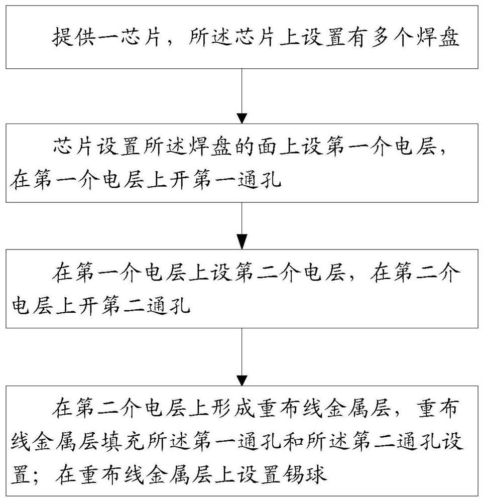
[0021] The application will be further described in detail below in conjunction with the accompanying drawings and embodiments. It should be understood that the specific embodiments described here are only used to explain related inventions, rather than to limit the invention. It should also be noted that, for ease of description, only parts related to the invention are shown in the drawings.

[0022] It should be noted that, in the case of no conflict, the embodiments in the present application and the features in the embodiments can be combined with each other. The present application will be described in detail below with reference to the accompanying drawings and embodiments.

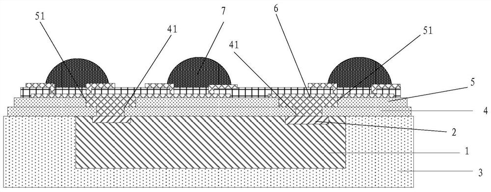
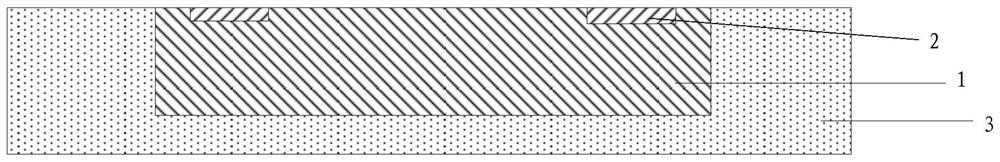
[0023] Please refer to figure 1 , this embodiment provides a fan-out packaging structure, including a chip 1, a plurality of pads 2 are arranged on the chip 1, and the surface of the chip 1 without the pads 2 is covered with a packaging material 3;

[0024] The first dielectric layer 4 is arrange...


PUM

PropertyMeasurementUnit
thicknessaaaaaaaaaa

Abstract

The invention discloses a fan-out type packaging structure and a packaging method, and the structure comprises a chip, the chip is provided with a plurality of bonding pads, a first dielectric layer is disposed on the surface, provided with the bonding pads, of the chip, and the first dielectric layer is provided with a first through hole; a second dielectric layer is arranged on the first dielectric layer, and a second through hole is formed in the second dielectric layer; and a rewiring metal layer is arranged on the second dielectric layer and fills the first through hole and the second through hole. According to the technical scheme provided by the embodiment of the invention, the first through hole formed in the first dielectric layer can be matched with a smaller input/output pin on the chip, and the second through hole formed in the second dielectric layer can increase the special current flux, so that the purpose of optimizing the product performance is further achieved; the two dielectric layers can eliminate the height limitation in the packaging process so as to meet the requirement of a product, meanwhile, the high dielectric layer height can effectively protect the front face of the chip, the front face stress received by the chip in the testing stage is avoided, and the product can be rapidly led in in the packaging process.

Description

technical field [0001] The present invention generally relates to the packaging field, and in particular to a fan-out packaging structure and a packaging method. Background technique [0002] Since light, thin and short have become the development direction of electronic consumer products, the wafer-level packaging process that can save materials and processes and reduce the size of components has become more and more common. [0003] In the packaging semiconductor industry, the existing FCCSP (Flip Chip Chip Scale Package, packaging a single chip) packaging process is generally accepted by end customers. Because the package height is limited by the height of the copper pillars, it is usually not acceptable to change the product structure. Contents of the invention [0004] In view of the above defects or deficiencies in the prior art, it is desired to provide a fan-out packaging structure and packaging method. [0005] In the first aspect, a fan-out packaging structure i...

Claims


Application Information

Patent Timeline
Patent Type & Authority Applications(China)
IPC IPC(8): H01L23/482H01L23/485H01L23/488H01L21/50
CPCH01L23/4824H01L23/485H01L23/488H01L24/02H01L21/50H01L2224/0231H01L2224/02379
Inventor 李尚轩
Owner NANTONG TONGFU MICROELECTRONICS CO LTD
Why Eureka
Try Eureka