Fingerprint identification area indicating device based on multi-color electrochromic structure and application of fingerprint identification area indicating device

A technology of fingerprint identification and indication device, applied in the optical or photoelectric field, can solve the problems affecting the integrity of electronic equipment, the sealing performance of the whole machine, etc., and achieve the effect of improving the integration and fingerprint identification efficiency and broad application prospects.

Active Publication Date: 2021-05-25
SUZHOU INST OF NANO TECH & NANO BIONICS CHINESE ACEDEMY OF SCI
View PDF4 Cites 0 Cited by
  • Summary
  • Abstract
  • Description
  • Claims
  • Application Information

AI Technical Summary

Problems solved by technology

However, slotting in the rear case will easily affect the integrity of t

Method used


Image

  • Fingerprint identification area indicating device based on multi-color electrochromic structure and application of fingerprint identification area indicating device
  • Fingerprint identification area indicating device based on multi-color electrochromic structure and application of fingerprint identification area indicating device
  • Fingerprint identification area indicating device based on multi-color electrochromic structure and application of fingerprint identification area indicating device

Examples


Embodiment 1

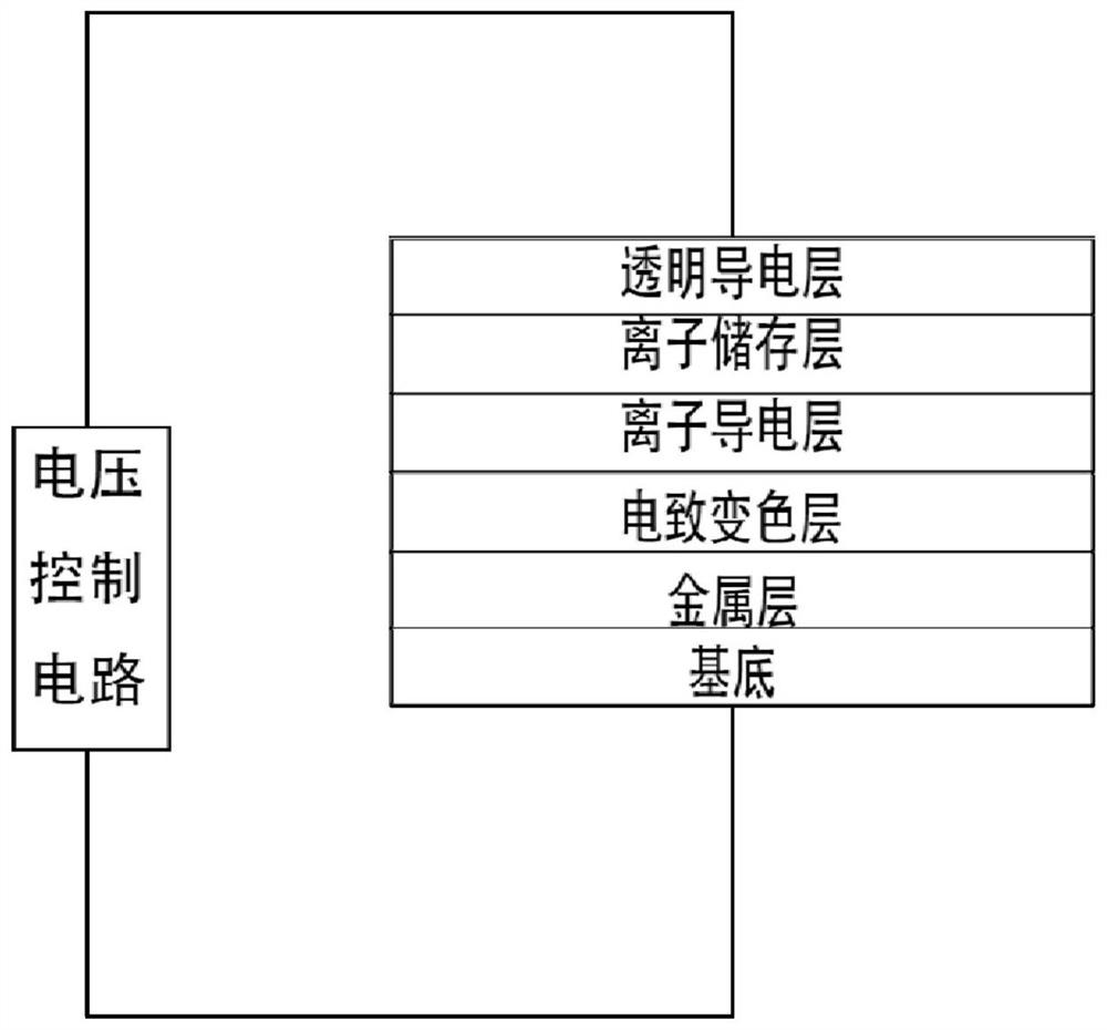
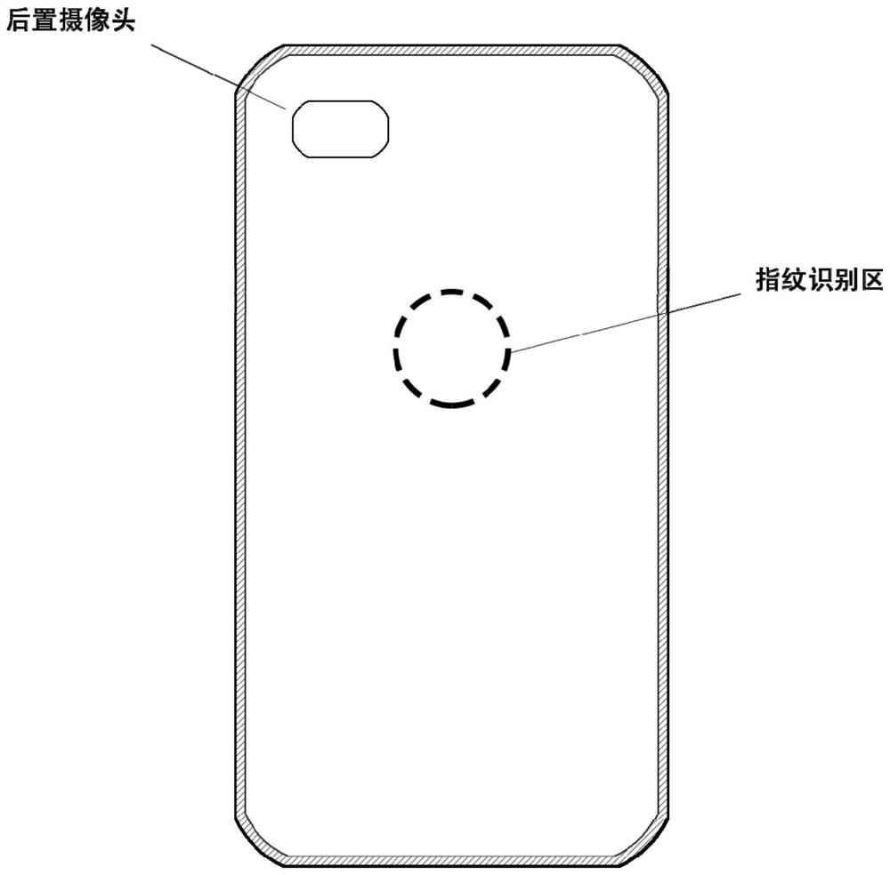
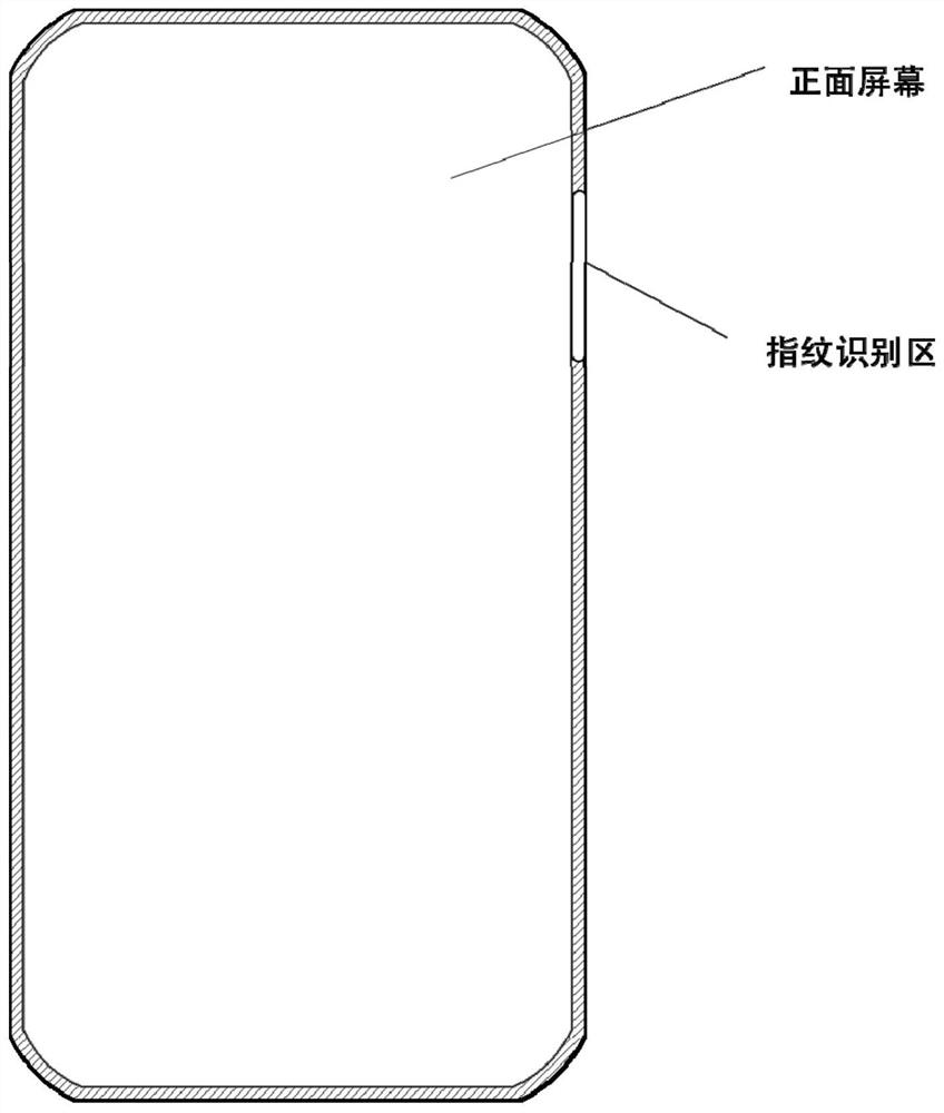
[0146] Embodiment 1 This embodiment discloses an electronic device based on a multi-color electrochromic structure fingerprint identification area indicator device, including a cover plate, a multi-color electrochromic structure, a fingerprint identification component, and, together with the multi-color electrochromic structure, A processor electrically connected to the fingerprint identification component; the processor can regulate the light transmittance of the colorful electrochromic structure, so that it is in an active state when the fingerprint identification component detects that a user's finger is approaching, so that the multi-color electrochromic structure The color change of the color electrochromic structure is different from the color of the cover plate, so as to indicate the position of the fingerprint recognition area, and when the fingerprint recognition component is in an inactive state, the color of the colorful electrochromic structure is consistent with the...

Embodiment 2

[0148] Embodiment 2 This embodiment discloses an electronic device based on a multi-color electrochromic structure fingerprint identification area indicator device, including a cover plate, a multi-color electrochromic structure, a fingerprint identification component, and, together with the multi-color electrochromic structure, A processor electrically connected to the fingerprint identification component; the processor can regulate the light transmittance of the colorful electrochromic structure, so that it is in an active state when the fingerprint identification component detects that a user's finger is approaching, so that the multi-color electrochromic structure The color change of the color electrochromic structure is different from the color of the cover plate, so as to indicate the position of the fingerprint recognition area, and when the fingerprint recognition component is in an inactive state, the color of the colorful electrochromic structure is consistent with the...

Embodiment 3

[0154] A working electrode of a colorful electrochromic structure provided in this embodiment includes a first optical structure layer, a second optical structure layer, a dielectric layer and a base layer, which can be referred to Image 6 shown.

[0155] Wherein, the first optical structure layer is air, the second optical structure is a metal tungsten (W) layer, the medium layer is formed of tungsten oxide, and the base layer may be PET film.

[0156] The preparation method of the working electrode of the colorful electrochromic structure is as follows: on a clean PET substrate, a layer of tungsten film is firstly sputtered by magnetron sputtering. Preferably, the thickness of the tungsten film is selectively sputtered to be about 10nm. Then a layer of tungsten oxide is sputtered on the tungsten film by magnetron sputtering. Preferably, the thickness of the tungsten oxide layer is set at 100nm-400nm.

[0157] Of course, the aforementioned tungsten film can also be prepare...


PUM

PropertyMeasurementUnit
Thicknessaaaaaaaaaa
Thicknessaaaaaaaaaa
Thicknessaaaaaaaaaa

Abstract

The invention discloses a fingerprint identification area indicating device based on a multi-color electrochromic structure and application of the fingerprint identification area indicating device. The fingerprint identification area indicating device comprises a cover plate, a multi-color electrochromic structure, a fingerprint identification assembly and a processor; the multi-color electrochromic structure comprises a working electrode, an electrolyte and a counter electrode; the working electrode comprises a first optical structure layer and a second optical structure layer which are opposite to each other and arranged in parallel, a dielectric layer is arranged between the first optical structure layer and the second optical structure layer, and the dielectric layer is made of electrochromic materials. The bonding interface of the dielectric layer and the first optical structure layer and the bonding interface of the dielectric layer andthe second optical structure layer are a first surface and a second surface of the dielectric layer respectively, and the first surface, the second surface and the dielectric layer form an optical cavity. According to the invention, by changing the color of the multi-color electrochromic structure, the position of the fingerprint identification area can be displayed, the voltage can be changed to present a specified color so as to maintain the color consistency of the appearance of the shell, and the integrity of the whole machine and the fingerprint identification efficiency are improved.

Description

technical field [0001] The invention relates to an electrochromic device, in particular to a fingerprint identification area indication device based on a multicolor electrochromic structure and a method for indicating a fingerprint identification area based on a multicolor electrochromic structure, belonging to the field of optical or photoelectric technology. Background technique [0002] At present, for rear fingerprints in electronic devices, the fingerprint identification module is generally placed by digging a groove in the rear cover, so as to indicate the position of the fingerprint identification area as a separate area. However, making a slot on the rear shell is likely to affect the integrity of the electronic device and the airtight performance of the whole machine. Contents of the invention [0003] The main purpose of the present invention is to provide a fingerprint identification area indication device based on a multicolor electrochromic structure and its a...

Claims


Application Information

Patent Timeline
IPC IPC(8): G02F1/155G02F1/157G02F1/153G02F1/163G06K9/00
CPCG02F1/155G02F1/157G02F1/1533G02F1/163G06V40/13
Inventor 赵志刚张曙陈健王振丛杉
Owner SUZHOU INST OF NANO TECH & NANO BIONICS CHINESE ACEDEMY OF SCI
Why Eureka
Try Eureka