Light-emitting panel and manufacturing method thereof

A light-emitting panel and light-shielding metal technology, which is applied in semiconductor/solid-state device manufacturing, electrical components, transistors, etc., can solve problems such as low yield rate and complex process technology of light-emitting diode display devices, so as to reduce etching times, improve process efficiency, The effect of simplifying the process difficulty

Active Publication Date: 2021-05-25
SHENZHEN CHINA STAR OPTOELECTRONICS SEMICON DISPLAY TECH CO LTD
View PDF6 Cites 5 Cited by
  • Summary
  • Abstract
  • Description
  • Claims
  • Application Information

AI Technical Summary

Problems solved by technology

[0004] This application provides a light-emitting panel and its manufacturing method to solve the technical problems of complex manufacturing process and low yield of existing light-emitting diode display devices

Method used


Image

  • Light-emitting panel and manufacturing method thereof
  • Light-emitting panel and manufacturing method thereof
  • Light-emitting panel and manufacturing method thereof

Examples


Embodiment Construction

[0042] The technical solutions in the embodiments of the present application will be clearly and completely described below in conjunction with the drawings in the embodiments of the present application. Apparently, the described embodiments are only some of the embodiments of this application, not all of them. Based on the embodiments in this application, all other embodiments obtained by those skilled in the art without making creative efforts belong to the scope of protection of this application.

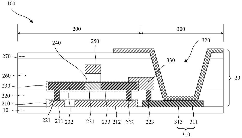
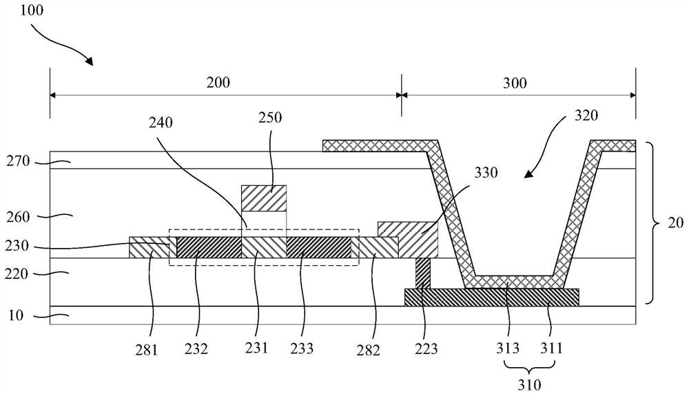
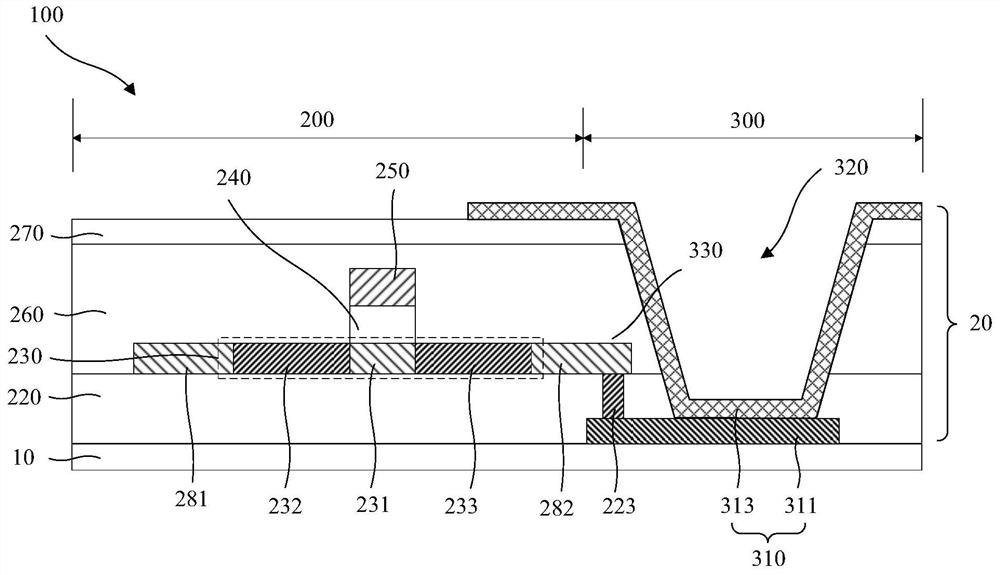
[0043] The driving circuit board in the existing light-emitting panel has a complicated manufacturing process, which usually requires 7 photomasks to complete the preparation process of the driving circuit board; at the same time, when performing the process of binding terminals, black light-shielding materials for blocking the semiconductor layer may be required. The contact with the binding terminal causes the black light-shielding material to remain on the binding terminal, wh...


PUM


Abstract

The invention provides a light-emitting panel and a manufacturing method thereof. The light-emitting panel comprises a thin film transistor area and a binding area away from the thin film transistor area, a plurality of thin film transistor units are arranged in the thin film transistor area, at least one first terminal is arranged in the binding area, and the first terminal at least comprises a first electrode located on the substrate. The first electrode and at least one of the first metal layer and the second metal layer in the thin film transistor unit are arranged on the same layer, so that the first electrode is electrically connected with the driving circuit layer through the electric connecting component; and the first electrode, the source and drain electrodes in the driving circuit layer and the shading metal are formed in the same process, so that the etching times of the manufacturing process are reduced, the process difficulty of the light-emitting panel is simplified, and the manufacturing efficiency is improved.

Description

technical field [0001] The present application relates to the display field, in particular to a light-emitting panel and a manufacturing method thereof. Background technique [0002] The backlight module of the existing light-emitting diode display devices usually includes a driving circuit board and light-emitting diodes on the driving circuit board, such as Micro LED or Mini LED, so the structural design of the backlight module is particularly important in high-resolution products. [0003] The driving circuit board in the existing backlight module has a complicated manufacturing process, which usually requires 7 photomasks to complete the preparation process of the driving circuit board; at the same time, when performing the process of binding terminals, a black light-shielding material for blocking the semiconductor layer is required It may be in contact with the binding terminal, resulting in black light-shielding material remaining on the binding terminal, affecting th...

Claims


Application Information

Patent Timeline
Patent Type & Authority Applications(China)
IPC IPC(8): H01L27/12H01L21/77H01L27/15H01L29/786H01L33/62
CPCH01L27/124H01L27/1259H01L29/78633H01L33/62H01L27/156H01L2933/0066
Inventor 刘俊领
Owner SHENZHEN CHINA STAR OPTOELECTRONICS SEMICON DISPLAY TECH CO LTD
Why Eureka
Try Eureka