Semiconductor structure and forming method thereof

A technology of semiconductor and isolation structure, applied in the field of semiconductor structure and its formation, can solve the problems of gate structure's poor control ability of channel and difficulty of channel, etc.

Active Publication Date: 2021-05-28
SEMICON MFG INT (SHANGHAI) CORP +1
View PDF9 Cites 0 Cited by
  • Summary
  • Abstract
  • Description
  • Claims
  • Application Information

AI Technical Summary

Problems solved by technology

However, as the channel length of the device shortens, the distance between the source and the drain of the device also shortens, so the ability of the gate structure to control the channel becomes worse, and the gate voltage pi

Method used


Image

  • Semiconductor structure and forming method thereof
  • Semiconductor structure and forming method thereof
  • Semiconductor structure and forming method thereof

Examples


Embodiment Construction

[0029] Currently formed devices still suffer from poor performance. The reasons for the poor performance of the device are analyzed in conjunction with a method of forming a semiconductor structure.

[0030] refer to Figure 1 to Figure 4 , shows a structural schematic diagram corresponding to each step in a method for forming a semiconductor structure.

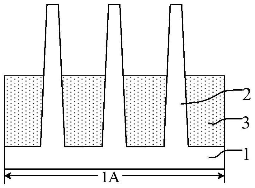
[0031] refer to figure 1 , provide a base, the base includes a first device region 1A for forming a first device and a second device region (not shown) for forming a second device, the base includes a substrate 1 and a substrate protruding from the substrate Initial fins 2 of bottom 1.

[0032] continue to refer figure 1 , forming an isolation structure 3 on the substrate exposed by the initial fin 2, the isolation structure 3 covers part of the sidewall of the initial fin 2, and the top surface of the isolation structure 3 is lower than the initial fin 2 top surface.

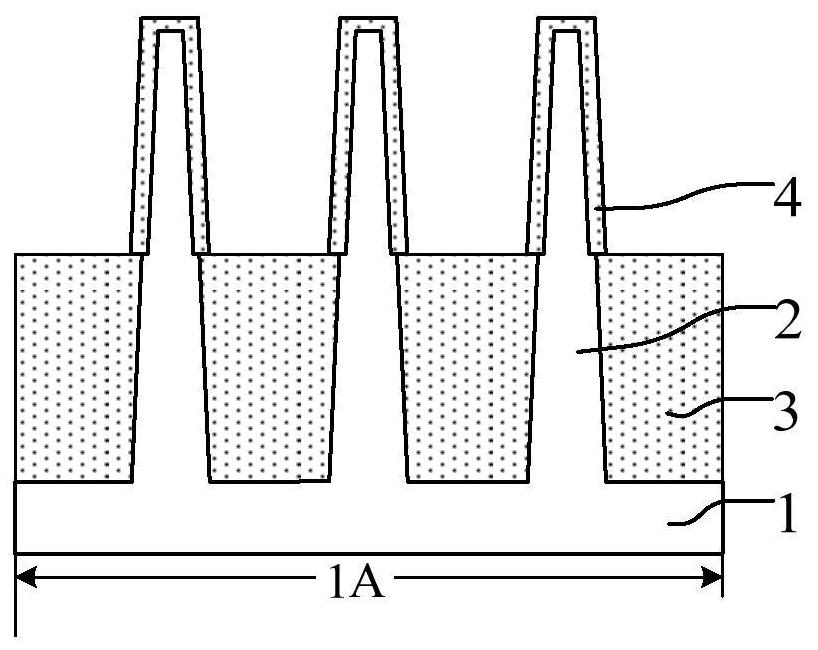
[0033] refer to figure 2 , performing a first o...


PUM


Abstract

The invention discloses a semiconductor structure and a forming method thereof. The method comprises the steps: providing a substrate which comprises a first device region and comprises a substrate and an initial fin part protruding out of the substrate; forming an isolation structure on the substrate exposed out of the initial fin part; forming an initial protection layer on the top surfaces of the isolation structure and the initial fin part and the side wall of the initial fin part exposed by the isolation structure; carrying out annealing treatment, so that the initial protection layer in contact with the isolation structure is converted into a sacrificial layer, and an unconverted initial protection layer on the top surface and the side wall of the initial fin part is used as a protection layer; removing the sacrificial layer of the first device region, and exposing a part of side wall, close to the isolation structure, of the initial fin part; taking the part, exposed by the protection layer and the isolation structure, of the initial fin part as an initial neck fin part; and thinning the side wall of the initial neck fin part in the first device region along the direction perpendicular to the extension direction of the initial fin part and the direction perpendicular to the side wall of the initial neck fin part to form the neck fin part. The embodiment of the invention is beneficial to improving the performance of the semiconductor structure.

Description

technical field [0001] Embodiments of the present invention relate to the field of semiconductor manufacturing, and in particular, to a semiconductor structure and a method for forming the same. Background technique [0002] In semiconductor manufacturing, with the development trend of ultra-large-scale integrated circuits, the feature size of integrated circuits continues to decrease. In order to adapt to smaller feature sizes, metal-oxide-semiconductor field-effect transistors (Metal-Oxide-Semiconductor Field-Effect Transistor , MOSFET) channel length has been shortened accordingly. However, as the channel length of the device is shortened, the distance between the source and the drain of the device is also shortened, so the control ability of the gate structure to the channel becomes worse, and the gate voltage pinches off (Pinch off) the channel. The channel becomes more and more difficult, making the phenomenon of subthreshold leakage (Subthreshold leakage), the so-cal...

Claims


Application Information

Patent Timeline
IPC IPC(8): H01L29/78H01L21/336
CPCH01L29/7855H01L29/66795
Inventor 渠汇
Owner SEMICON MFG INT (SHANGHAI) CORP
Why Eureka
Try Eureka