
Chip detection method, electronic equipment and storage medium

A technology for chip detection and chip-to-be-test, which is applied in measuring devices, optical testing of flaws/defects, and material analysis through optical means, and can solve problems such as reducing the efficiency of defect analysis and processing, unrecognizable defects, and indistinct features of defects , to achieve the effect of improving processing efficiency, improving efficiency, and reducing data collection costs

Pending Publication Date: 2021-06-01
高视科技(苏州)股份有限公司
View PDF5 Cites 2 Cited by
  • Summary
  • Abstract
  • Description
  • Claims
  • Application Information

AI Technical Summary

Problems solved by technology

[0004] 1. The chip is only amplified once, which is equivalent to indiscriminately amplifying all defects on the chip. Considering that the characteristics of different types of defects need to be accurately identified under different magnifications, this detection method will cause The characteristics of some defects are not obvious, resulting in identification errors or failure to identify, thus affecting the over-missing rate of equipment;
[0005] 2. The high-magnification magnification of the chip makes the field of view of the captured image very limited. In the case of the same chip area, more photos need to be taken to obtain the defect image, the processing process is complicated, and the acquisition cost of obtaining and analyzing the image increases. It also increases the burden of data transmission and storage, resulting in low efficiency of defect analysis and processing, especially in the case of various and complex defects, which further reduces the efficiency of defect analysis and processing

Method used


Image

  • Chip detection method, electronic equipment and storage medium
  • Chip detection method, electronic equipment and storage medium
  • Chip detection method, electronic equipment and storage medium

Examples


Embodiment 1

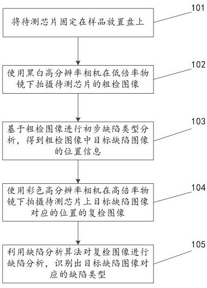
[0052] figure 1 It is a schematic flowchart of Embodiment 1 of the chip detection method shown in the embodiment of the present application.

[0053] see figure 1 , Embodiment 1 of the chip detection method in the embodiment of the present application includes:

[0054] 101. Fix the chip to be tested on the sample placement plate;

[0055] The chip to be tested is an LED chip, which can be a traditional LED chip, a mini LED chip or a micro LED chip, and is especially suitable for a micro LED chip.

[0056] The sample placement plate is used to fix the LED chip to be tested, and can drive the LED chip to be tested to move quickly, and prevent the chip to be tested from shifting during the moving process, that is, to prevent the chip to be tested from being relative to the sample placement plate. The position changes; the surface of the sample placement plate can be treated with black frosting to prevent reflection from affecting imaging.

[0057] In this embodiment, the way...

Embodiment 2

[0080] In order to facilitate understanding, an embodiment of the chip detection method is provided below for description. In the first embodiment above, after the chip to be tested is fixed on the sample placement plate, it is necessary to adjust the placement angle of the chip to be tested and complete the focusing operation. In order to ensure the effect of subsequent image capture.

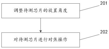
[0081] figure 2 It is a schematic flowchart of Embodiment 2 of the chip detection method shown in the embodiment of the present application.

[0082] see figure 2 , Embodiment 2 of the chip detection method in the embodiment of the present application includes:

[0083] 201. Adjust the placement angle of the chip to be tested;

[0084] Adjust the angle so that the long and short sides of the chip to be tested are parallel to the XY axis of the camera. It can be that the long side of the chip to be tested is parallel to the X axis of the camera, and the short side is parallel to the Y axis...

Embodiment 3

[0099] For ease of understanding, an example of the chip inspection method is provided below for illustration. In the first embodiment above, the preliminary defect type analysis based on the rough inspection image needs to classify the defect images in the rough inspection image, and classify images are processed differently.

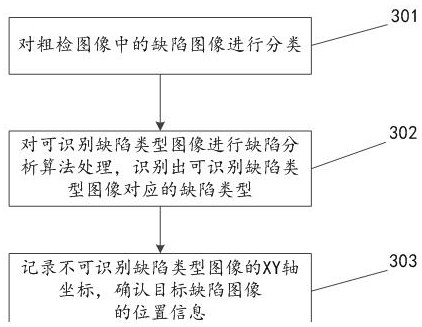
[0100] image 3 It is a schematic flowchart of Embodiment 3 of the chip detection method shown in the embodiment of the present application.

[0101] see image 3 , Embodiment 3 of the chip detection method in the embodiment of the present application includes:

[0102] 301. Classify the defect images in the rough inspection images;

[0103] A deep convolutional neural network algorithm is used to classify the defect images in the rough inspection images into identifiable defect type images and unrecognizable defect type images.

[0104] The deep convolutional neural network algorithm is a kind of feed-forward neural network algorithm that includes...


PUM


Abstract

The invention relates to a chip detection method, electronic equipment and a storage medium. The method comprises the following steps: using a black and white high-resolution camera to shoot a rough detection image of a to-be-detected chip under a low-magnification objective lens; performing preliminary defect type analysis based on the rough detection image; using a color high-resolution camera to shoot an upper surface image and a lower surface image of the to-be-detected chip under a high-magnification objective lens; fusing the upper surface image and the lower surface image into one image by using an image fusion algorithm to obtain a recheck image with superimposed depth-of-field information; and performing defect analysis on the reinspection image by using a defect analysis algorithm, and identifying a defect type corresponding to the target defect image. According to the scheme provided by the invention, the black and white high-resolution camera can be used for completing rough inspection under the low-magnification objective lens, and the color high-resolution camera can be used for completing reinspection under the high-magnification objective lens, so that the data acquisition cost for acquiring the to-be-analyzed image in the early stage is reduced, and the efficiency of the whole defect analysis and treatment process is improved.

Description

technical field [0001] The present application relates to the technical field of chip detection, in particular to a chip detection method, electronic equipment and a storage medium. Background technique [0002] With the rapid development of various smart devices, the miniaturization of devices in smart devices has also become a major trend. Among them, the LED chips used in the screen are closely related to the resolution of the screen: when other conditions remain unchanged, the smaller the LED chip, the higher the resolution of the screen. On this basis, micron LED chips came into being. Micron LEDs are extremely small in size, generally only 20-30 microns (traditional LED chips: >1000 microns, mini LED chips: 100-200 microns). [0003] Micron LED chip is a new generation of chip, and its corresponding detection equipment is less. Now the commonly used equipment is to modify the detection equipment of mini LED chip, and simply increase the magnification of the chip b...

Claims


Application Information

Patent Timeline
Patent Type & Authority Applications(China)
IPC IPC(8): G01N21/88
CPCG01N21/8851G01N2021/8887
Inventor 石圣涛蒋贵和王巧彬
Owner 高视科技(苏州)股份有限公司
Learn More