Photoelectric material and device appearance detection system

A photoelectric material and appearance inspection technology, which is applied in the direction of material analysis, material analysis, and optical testing for flaws/defects through optical means, can solve the problems of accuracy impact, cumbersome process, and low efficiency, and achieve easy operation and understanding, Simple structure and improved test efficiency

Pending Publication Date: 2021-06-04
成都市产品质量监督检验研究院
View PDF7 Cites 0 Cited by
  • Summary
  • Abstract
  • Description
  • Claims
  • Application Information

AI Technical Summary

Problems solved by technology

Therefore, this conventional detection method requires the tester to repeat the action many times and record it in paper to complete the test content, which has the disadvantages of cumbersome

Method used


Image

  • Photoelectric material and device appearance detection system

Examples


Embodiment Construction

[0018] The following will clearly and completely describe the technical solutions in the embodiments of the present invention with reference to the accompanying drawings in the embodiments of the present invention. Obviously, the described embodiments are only some, not all, embodiments of the present invention. Based on the embodiments of the present invention, all other embodiments obtained by persons of ordinary skill in the art without making creative efforts belong to the protection scope of the present invention.

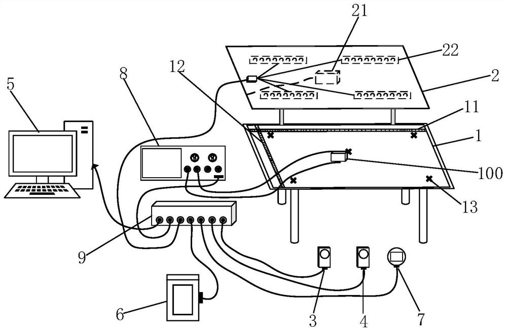
[0019] refer to figure 1 , the optoelectronic material and device appearance detection system of the embodiment of the present invention includes a detection platform 1, a mobile platform 2, an irradiance meter 3, an illuminance meter 4 and a data processing terminal 5, and the detection platform 1 is used to place the photoelectric material and device to be tested 100, the surface of the detection platform 1 is provided with a horizontal length scale 11 and a...


PUM


Abstract

The invention discloses a photoelectric material and a device appearance detection system. Thephotoelectric material and device appearance detection system disclosed by the present invention comprises a detection table, a mobile pan-tilt, an irradiance meter, an illuminometer and a data processing terminal; the detection table is used for placing a photoelectric material and a device to be detected; the surface of the detection table is provided with a transverse length scale and a longitudinal width scale; the mobile pan-tilt is suspended above the detection table, and can vertically and horizontally move relative to the detection table; a camera and a plurality of light supplementing lamps distributed around the camera are arranged below the movable pan-tilt; the irradiance meter is used for collecting the irradiance of the detection table; the illuminometer is used for collecting the illuminance of the detection table; and the data processing terminal is connected with the irradiance meter, the illuminometer, the camera and each light supplementing lamp, and is used for adjusting the focal length of the camera and the brightness of each light supplementing lamp, and obtaining pictures shot by the camera, the irradiance collected by the irradiance meter and the illuminance collected by the illuminometer. According to the invention, the labor cost and time cost of detection can be greatly reduced, and the working efficiency and accuracy are greatly improved.

Description

technical field [0001] The invention relates to the technical field of appearance inspection, in particular to a photoelectric material and device appearance inspection system. Background technique [0002] At present, the appearance inspection of optoelectronic materials and devices is to check whether there are defects in the appearance of optoelectronic materials and devices by manual "visual inspection" under conventional requirements, and record the appearance defects of optoelectronic materials and devices by taking pictures. During the inspection process, the testers need to conduct repeated "visual" inspections on various parts of the optoelectronic materials and devices, and repeatedly "photograph" records to mark the appearance defects of optoelectronic materials and devices. Therefore, this conventional detection method requires testers to repeat actions many times and record them on paper to complete the test content, which has the disadvantages of cumbersome pro...

Claims


Application Information

Patent Timeline
IPC IPC(8): G01N21/88
CPCG01N21/8806
Inventor 李国贵任麟东李添江瑜夏庚培成皓楠向维
Owner 成都市产品质量监督检验研究院
Why Eureka
Try Eureka