
Eureka
For R&D, Eureka makes reading and utilizing patents & technical documents easy.
Eureka AIR
Designed for self-driven R&D workflows. Generate viable solutions, solve complex R&D challenges, empower your innovation with AI.

Eureka Materials
Designed for material experts only. Revolutionize your material R&D, from search, analyze, to developing new materials.

TechResearch
Generate reliable direction feasibility study reports for your R&D in just a few steps.

TechSeek
Discover and master advanced knowledge NOW. Basics, ideas, possibilities, all at once.

TechMind
As an expert in R&D Theories, TechMind can generates customized viable solutions instantly.

TechRisk
Analyze your overall solution with one click, know your potential R&D risks in advance.

TechMonitor
Get weekly tech updates, stay abreast of the latest tech innovations and key insights.
Wrap-around gate assembly and manufacturing method thereof
A wrap-around, gate technology, applied in semiconductor/solid-state device manufacturing, electrical components, semiconductor devices, etc., can solve the problems of losing the advantages of compound semiconductors and not being able to obtain high current gain characteristics
- Summary
- Abstract
- Description
- Claims
- Application Information
AI Technical Summary
Problems solved by technology
Method used
Image

Examples
Embodiment Construction
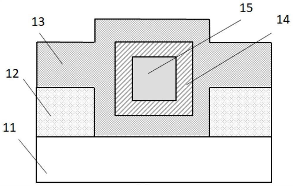
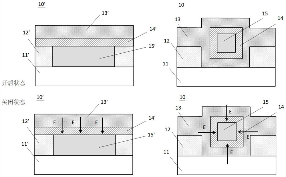
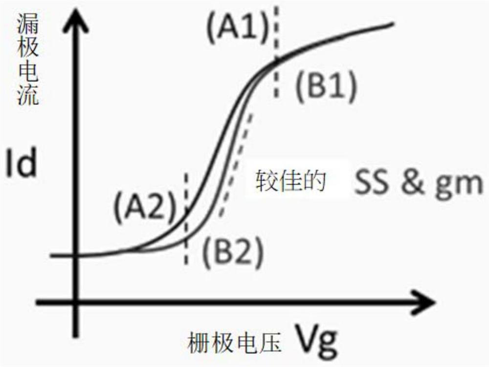
[0012] In order to make the purpose, technical features and advantages of the present invention more understandable to those in the relevant technical field, and to implement the present invention, the technical features and implementation modes of the present invention are specifically explained in conjunction with the attached drawings, and listed The preferred embodiment is further described. The diagrams compared below are intended to express the schematic representations related to the features of the present invention, and do not need to be completely drawn according to the actual situation. The description about the implementation of this case involves technical content well known to those skilled in the art, and will not be stated again.
[0013] In the present invention, the x-axis, y-axis and z-axis adopt a right-handed Cartesian coordinate system, that is, a three-axis orthogonal (x, y, z) coordinate system. The detailed directions of the x-axis, y-axis, z-axis and...
PUM
| Property | Measurement | Unit |
|---|---|---|
| width | aaaaa | aaaaa |
| height | aaaaa | aaaaa |
| thickness | aaaaa | aaaaa |
Abstract
Description
Claims
Application Information
 - R&D Engineer
- R&D Manager
- IP Professional
- Industry Leading Data Capabilities
- Powerful AI technology
- Patent DNA Extraction
Browse by: Latest US Patents, China's latest patents, Technical Efficacy Thesaurus, Application Domain, Technology Topic, Popular Technical Reports.
© 2024 PatSnap. All rights reserved.Legal|Privacy policy|Modern Slavery Act Transparency Statement|Sitemap|About US| Contact US: help@patsnap.com