
Forming method of transistor device layout

A transistor and layout technology, which is applied in the field of transistor device layout formation, can solve the problem of high power consumption in shadowed areas, and achieve the effects of reducing power consumption, avoiding shadowed areas, and reducing leakage

Pending Publication Date: 2021-06-08
SHANGHAI HUAHONG GRACE SEMICON MFG CORP
View PDF0 Cites 1 Cited by
  • Summary
  • Abstract
  • Description
  • Claims
  • Application Information

AI Technical Summary

Problems solved by technology

[0003] The purpose of the present invention is to provide a method for forming the layout of a transistor device, so as to solve the problems of shadow areas and large power consumption in the existing transistor devices

Method used


Image

  • Forming method of transistor device layout
  • Forming method of transistor device layout
  • Forming method of transistor device layout

Examples


Embodiment Construction

[0033] The method for forming the transistor device layout proposed by the present invention will be further described in detail below in conjunction with the accompanying drawings and specific embodiments. The advantages and features of the present invention will become clearer from the following description. It should be noted that all the drawings are in a very simplified form and use imprecise scales, and are only used to facilitate and clearly assist the purpose of illustrating the embodiments of the present invention.

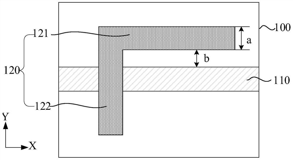
[0034] The inventors found that the reason why there is a shaded area in the active region of the existing transistor device is that in the manufacturing method of the transistor device, ion implantation is usually performed on the active region of the transistor device to form the source region and the drain region , if the distance between the first part of the floating gate and the active area is close, the first part of the floating gate will block th...


PUM

PropertyMeasurementUnit
Sizeaaaaaaaaaa

Abstract

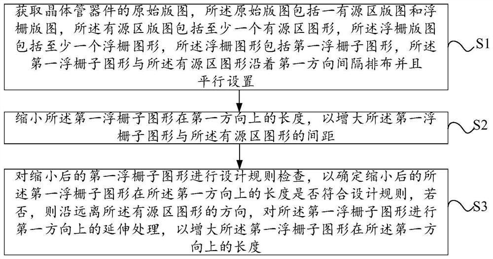
The invention provides a forming method of a transistor device layout. The forming method is characterized in that the distance between a first floating gate pattern and an active region pattern is increased by shortening the length of the first floating gate pattern in a first direction, so that in a manufacturing process of a transistor device, the distance between a floating gate formed by adopting the floating gate pattern and an active region formed by adopting the active region pattern can be increased, so that a shadow region can be avoided, electric leakage can be reduced, and the power consumption of a transistor device can be reduced; and design rule check is carried out on the reduced first floating gate pattern to determine whether the length of the reduced first floating gate pattern in the first direction accords with a design rule, if not, extension processing is carried out on the first floating gate pattern in the first direction along a direction far away from the active region pattern, so that the length of the first floating gate pattern in the first direction is increased, and the situation that the size of the floating gate in the manufacturing process corresponding to the floating gate pattern is too small can be avoided.

Description

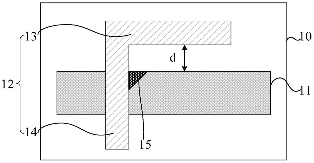
technical field [0001] The invention relates to the technical field of semiconductor manufacturing, in particular to a method for forming a transistor device layout. Background technique [0002] refer to figure 1 , which is a structural schematic diagram of a transistor device in the prior art. Such as figure 1 As shown, the existing transistor device includes: a substrate 10, an active region 11 located in the substrate 10, and a floating gate 12 located on the active region 11, and the floating gate 12 includes a first part 13 and the second portion 14, the first portion 13 of the floating gate 12 is perpendicular to the second portion 14, and the first portion 13 of the floating gate 12 is parallel to the active region 11, the second portion of the floating gate 12 14 covers a part of the active region 11, but there is a shadow region 15 in the active region 11, and the shadow region 15 will cause electric leakage and make the power consumption of the transistor devic...

Claims


Application Information

Patent Timeline
IPC IPC(8): H01L29/66H01L29/40H01L21/027H01L29/423
CPCH01L29/66409H01L29/401H01L21/027H01L29/42324
Inventor 孙访策郑舒静林晓帆黄冲张明
Owner SHANGHAI HUAHONG GRACE SEMICON MFG CORP
Learn More