Reverse analysis method for anomalies of patterned substrate LED epitaxial wafer

A technology for LED epitaxial wafers and patterned substrates, used in electrical components, circuits, semiconductor/solid-state device testing/measurement, etc., can solve the problem of lack of analysis methods, improve and optimize processes, expand analysis methods, and reduce abnormal products. Effect

Active Publication Date: 2021-06-11
广东中图半导体科技股份有限公司
View PDF4 Cites 0 Cited by
  • Summary
  • Abstract
  • Description
  • Claims
  • Application Information

AI Technical Summary

Problems solved by technology

The existing epitaxial wafer anomaly analysis methods mainly focus on the crystal quality of the epitaxial layer, but there are very few analysis methods that directly connect the pattern substrate with the epitaxial layer on it, resulting in some problems in engineering research or mass production. Epitaxy anomalies caused by patterned substrates are difficult to determine the cause

Method used


Image

  • Reverse analysis method for anomalies of patterned substrate LED epitaxial wafer
  • Reverse analysis method for anomalies of patterned substrate LED epitaxial wafer
  • Reverse analysis method for anomalies of patterned substrate LED epitaxial wafer

Examples


Embodiment Construction

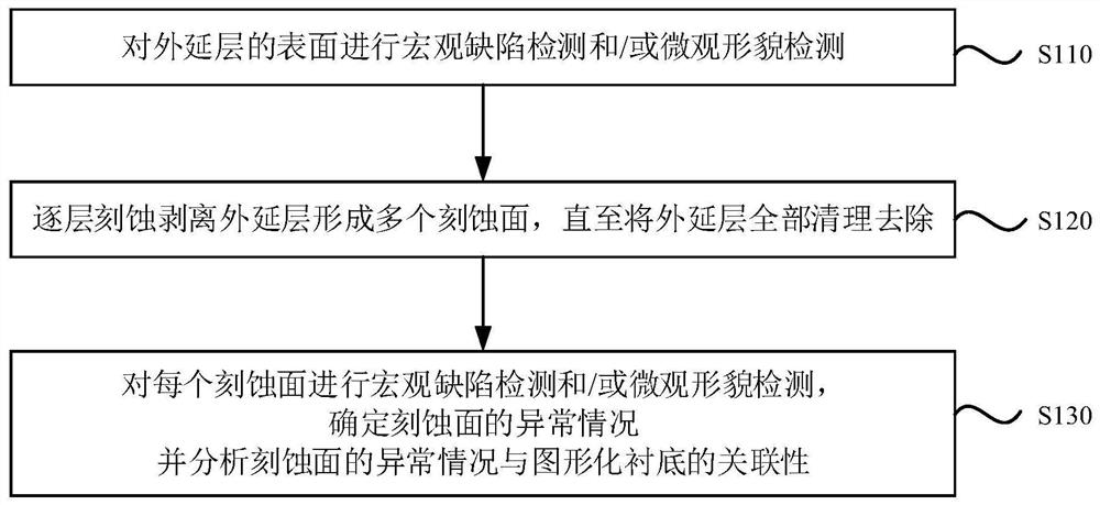
[0031] The present invention will be further described in detail below in conjunction with the accompanying drawings and embodiments. It should be understood that the specific embodiments described here are only used to explain the present invention, but not to limit the present invention. In addition, it should be noted that, for the convenience of description, only some structures related to the present invention are shown in the drawings but not all structures.

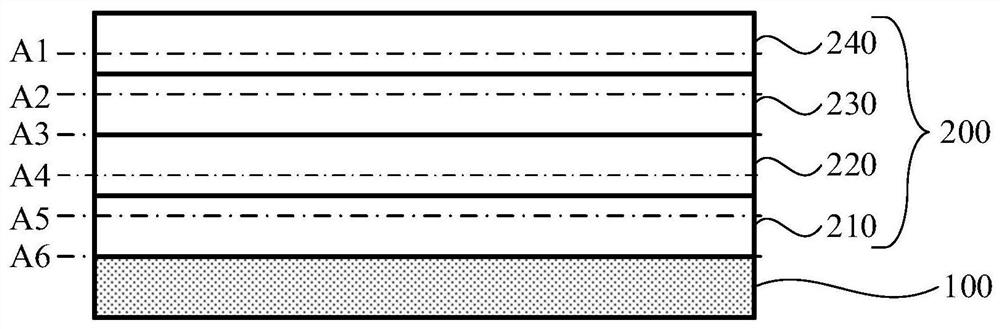
[0032] The patterned substrate LED epitaxial wafer provided by the embodiment of the present invention includes a patterned substrate and an epitaxial layer that are stacked. figure 1 It is a flow chart of a reverse analysis method for the abnormality of patterned substrate LED epitaxial wafers provided by the embodiment of the present invention. Such as figure 1 As shown, the reverse analysis method for the abnormality of the patterned substrate LED epitaxial wafer includes:

[0033] S110 , performing macroscop...


PUM


Abstract

The embodiment of the invention discloses a reverse analysis method for anomalies of a patterned substrate LED epitaxial wafer. The LED epitaxial wafer comprises a patterned substrate and an epitaxial layer which are arranged in a laminated manner. The reverse analysis method for anomalies of the patterned substrate LED epitaxial wafer comprises the following steps of carrying out macroscopic defect detection and / or microstructure detection on the surface of the epitaxial layer; etching and stripping the epitaxial layer layer by layer to form a plurality of etching surfaces until the epitaxial layer is completely cleaned and removed; and carrying out macroscopic defect detection and / or microstructure detection on each etching surface, determining the abnormal condition of the etching surface, and analyzing the relevance between the abnormal condition of the etching surface and the patterned substrate. According to the embodiment of the invention, the epitaxial layer is analyzed through layer-by-layer etching, so that the visual relation between the patterned substrate and the abnormity of the epitaxial layer can be established, the process technology can be improved and optimized, abnormal products are reduced, and the product quality is improved.

Description

technical field [0001] Embodiments of the present invention relate to optoelectronic technology, and in particular to a reverse analysis method for abnormalities of patterned substrate LED epitaxial wafers. Background technique [0002] Patterned sapphire substrate is currently the most important substrate material for epitaxial growth of GaN LEDs. The microstructure and optical parameters of its surface pattern have a great influence on the quality of epitaxial wafers, such as the same periodic arrangement of different bottom widths. There is a big difference in the luminance of the patterned sapphire substrate after the same epitaxial process. The existing epitaxial wafer anomaly analysis methods mainly focus on the crystal quality of the epitaxial layer, but there are very few analysis methods that directly connect the pattern substrate with the epitaxial layer on it, resulting in some problems in engineering research or mass production. Epitaxy anomalies caused by patte...

Claims


Application Information

Patent Timeline
Patent Type & Authority Applications(China)
IPC IPC(8): H01L21/66
CPCH01L22/12H01L22/24Y02P70/50
Inventor 曾广艺张剑桥王子荣陆前军
Owner 广东中图半导体科技股份有限公司
Why Eureka
Try Eureka