Photon matrix vector multiplier

A matrix-vector and multiplier technology, applied in the field of optical information, can solve problems such as difficult large-scale expansion and sensitive process errors, and achieve the effect of easy basic structure, easy scale expansion, and large process tolerance

Active Publication Date: 2021-06-18
XI'AN INST OF OPTICS & FINE MECHANICS - CHINESE ACAD OF SCI +2
View PDF15 Cites 0 Cited by
  • Summary
  • Abstract
  • Description
  • Claims
  • Application Information

AI Technical Summary

Problems solved by technology

[0004] The purpose of the present invention is to solve the problem that the existing photon matrix vector multiplier i

Method used


Image

  • Photon matrix vector multiplier
  • Photon matrix vector multiplier
  • Photon matrix vector multiplier

Examples


Example Embodiment

[0029] Example 1

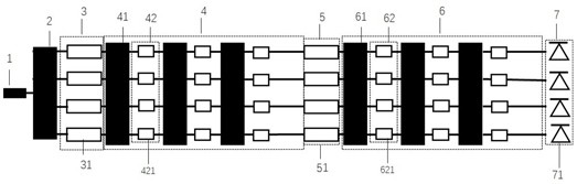
[0030] figure 2Shown is a schematic structural diagram of Embodiment 1 of the present invention. The photon matrix vector multiplier includes a light source 1, an input beam splitter 2, an input modulator array 3, a first multi-order diffraction network 4, an intermediate modulator array 5, The second multi-order diffractive network 6 and the detector array 7 . The light source 1 is connected to the input port of the input beam splitter 2 through a waveguide, the light energy of the light source 1 is divided into four parts by the input beam splitter 2, and the input modulator array 3 includes four first modulators 31, each first modulator 31 The input ports are respectively connected to the output ports of the input beam splitter 2 , the intermediate modulator array 5 includes four second modulators 51 ; the detector array 7 includes four detectors 71 . The first multi-stage diffraction network 4 includes five first photon distribution units, each of whi...

Example Embodiment

[0031] Embodiment 2

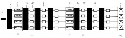
[0032] image 3 Shown is a schematic structural diagram of the second embodiment of the photonic matrix-vector multiplier of the present invention. In this embodiment, the first modulator 31 and the second modulator 51 both use electro-absorption modulators, and other parts are the same as those of the first embodiment.

Example Embodiment

[0033] Embodiment 3

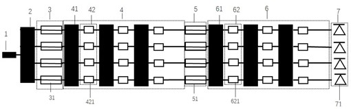
[0034] Figure 4 Shown is a schematic structural diagram of the third embodiment of the photonic matrix-vector multiplier according to the present invention. In this embodiment, the first modulator 31 and the second modulator 51 are both MEMS modulators, and other parts are the same as those of the first embodiment.


PUM


Abstract

The invention provides a photon matrix vector multiplier which solves the problems that an existing photon matrix vector multiplier is sensitive to process errors and is difficult to expand on a large scale. The photon matrix vector multiplier comprises a light source, an input beam splitter, an input modulator array, a first multi-stage diffraction network, an intermediate modulator array, a second multi-stage diffraction network and a detector array which are arranged in sequence, the input modulator array comprises N first modulators; the intermediate modulator array comprises N second modulators; the detector array comprises N detectors; the first multi-stage diffraction network comprises M stages of first photon distribution units, each stage of first photon distribution unit comprises a first optical splitter and a first phase modulator array, the second multi-stage diffraction network comprises M stages of second photon distribution units, and each stage of second photon distribution unit comprises a second optical splitter and a second phase modulator array. The structure provided by the invention has the advantages of being insensitive to process errors, high in realizability, easy to integrate and the like.

Description

technical field [0001] The invention relates to the technical field of optical information, in particular to a photon matrix vector multiplier. Background technique [0002] Computing technology is the core of modern information technology. Traditional electronic computing methods have the disadvantages of high energy consumption, low efficiency, and low parallelism, but photonic computing technology can overcome the above shortcomings. Matrix-vector multiplication is an important branch of photonic computing. [0003] For applications such as artificial intelligence, matrix-vector multiplication accounts for more than 90% of the total computation. The traditional on-chip photon vector matrix multiplier is based on a multi-stage Marzendel interferometer structure. Based on the principle of eigenvalue decomposition, the structure decomposes any matrix into a concatenated structure of two unitary matrices and a diagonal matrix, and realizes the unitary matrix through the Mac...

Claims


Application Information

Patent Timeline
IPC IPC(8): G06F7/523G06F17/16
CPCG06F7/523G06F17/16
Inventor 徐之光程东赵卫姚宏鹏杜炳政布兰特·埃弗雷特·李特尔罗伊·戴维森臧大伟张佩珩谭光明
Owner XI'AN INST OF OPTICS & FINE MECHANICS - CHINESE ACAD OF SCI
Why Eureka
Try Eureka