Mass transfer method for micro light-emitting diode chips

A technology of micro-light-emitting diodes and transfer methods, which is applied in the manufacture of electrical components, electric solid-state devices, semiconductor/solid-state devices, etc. simple craftsmanship

Active Publication Date: 2021-06-18
CHONGQING KONKA PHOTOELECTRIC TECH RES INST CO LTD
View PDF8 Cites 6 Cited by
  • Summary
  • Abstract
  • Description
  • Claims
  • Application Information

AI Technical Summary

Problems solved by technology

[0005] In view of the deficiencies in the prior art above, the purpose of this application is to provide a mass transfer method for micro-light-emitting diode chips, aiming to solve the problems of complex process and difficult implementation of the mass transfer method

Method used


Image

  • Mass transfer method for micro light-emitting diode chips
  • Mass transfer method for micro light-emitting diode chips
  • Mass transfer method for micro light-emitting diode chips

Examples


Embodiment Construction

[0036] In order to facilitate the understanding of the present application, the present application will be described more fully below with reference to the relevant drawings. Preferred embodiments of the application are shown in the accompanying drawings. However, the present application can be embodied in many different forms and is not limited to the embodiments described herein. On the contrary, the purpose of providing these embodiments is to make the disclosure of the application more thorough and comprehensive.

[0037] Unless otherwise defined, all technical and scientific terms used herein have the same meaning as commonly understood by one of ordinary skill in the technical field to which this application belongs. The terminology used herein in the description of the application is only for the purpose of describing specific embodiments, and is not intended to limit the application.

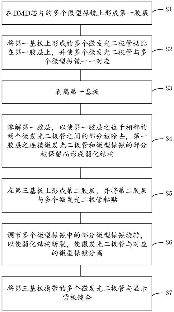
[0038] The current mass transfer technology of micro-LED chips has the problems o...


PUM


Abstract

The invention discloses a mass transfer method for micro light-emitting diode chips. The mass transfer method comprises the following steps: forming a first adhesive layer on a plurality of micro galvanometers of a DMD chip; bonding a plurality of micro light emitting diode chips formed on a first substrate on the first adhesive layer, and enabling the plurality of micro light emitting diode chips to be in one-to-one correspondence with a plurality of micro galvanometers; stripping the first substrate; dissolving the first adhesive layer to remove the part of the first adhesive layer between the two adjacent micro light emitting diode chips, and reserving the part of the first adhesive layer connecting the micro light emitting diode chips and the micro galvanometer to form a weakening structure; forming a second adhesive layer on a third substrate, and bonding the second adhesive layer with the plurality of micro light emitting diode chips; adjusting part of the plurality of micro galvanometers to rotate so as to break the weakening structure and separate the micro light emitting diode chips from the corresponding micro galvanometers; bonding the plurality of micro light emitting diode chips carried by the third substrate with the display back plate, wherein the transfer process is simple and easy to implement.

Description

technical field [0001] The invention relates to the technical field of transfer of micro-light emitting diode chips, in particular to a mass transfer method of micro-light-emitting diode chips. Background technique [0002] The Micro-LED display panel is a display device with tens of millions of micro-LED chips. The Micro-LED chip display panel has many advantages and has a good development prospect. [0003] In the manufacturing process of the micro-LED chip display panel, it is a key technology to transfer the huge amount of micro-LED chips formed on the substrate to the display backplane. The current mass transfer technology mainly includes solution method, laser selective dissolving method, etc., all of which have the problems of complicated process and difficult implementation. [0004] Therefore, how to provide a mass transfer method with simple process and easy implementation is an urgent problem to be solved. Contents of the invention [0005] In view of the abov...

Claims


Application Information

Patent Timeline
Patent Type & Authority Applications(China)
IPC IPC(8): H01L21/683H01L33/48
CPCH01L21/6835H01L33/48H01L2221/68386H01L2933/0033
Inventor 张嘉修锺光韦江仁杰
Owner CHONGQING KONKA PHOTOELECTRIC TECH RES INST CO LTD
Why Eureka
Try Eureka