
Micro light-emitting diode display panel, preparation method thereof and display device

A micro-light-emitting diode and display panel technology, which is applied in the direction of electrical components, electric solid-state devices, circuits, etc., can solve the problems affecting the display quality of the micro-light-emitting diode display panel and reduce the contrast of the micro-light-emitting diode display panel, so as to improve the display quality, Effects that reduce reflections and increase contrast

Inactive Publication Date: 2021-06-18
SHENZHEN CHINA STAR OPTOELECTRONICS SEMICON DISPLAY TECH CO LTD
View PDF7 Cites 1 Cited by
  • Summary
  • Abstract
  • Description
  • Claims
  • Application Information

AI Technical Summary

Problems solved by technology

[0004] An embodiment of the present invention provides a micro light-emitting diode display panel, which is used to solve the problem of micro-lights caused by the reflection of light from the source of the micro-light-emitting diode display panel in the prior art, the negative pole of the power line, and a plurality of metal wiring pads in the peripheral wiring area. The contrast ratio of the light-emitting diode display panel is reduced, which affects the technical problem of the display quality of the micro-light-emitting diode display panel

Method used


Image

  • Micro light-emitting diode display panel, preparation method thereof and display device
  • Micro light-emitting diode display panel, preparation method thereof and display device
  • Micro light-emitting diode display panel, preparation method thereof and display device

Examples


Embodiment Construction

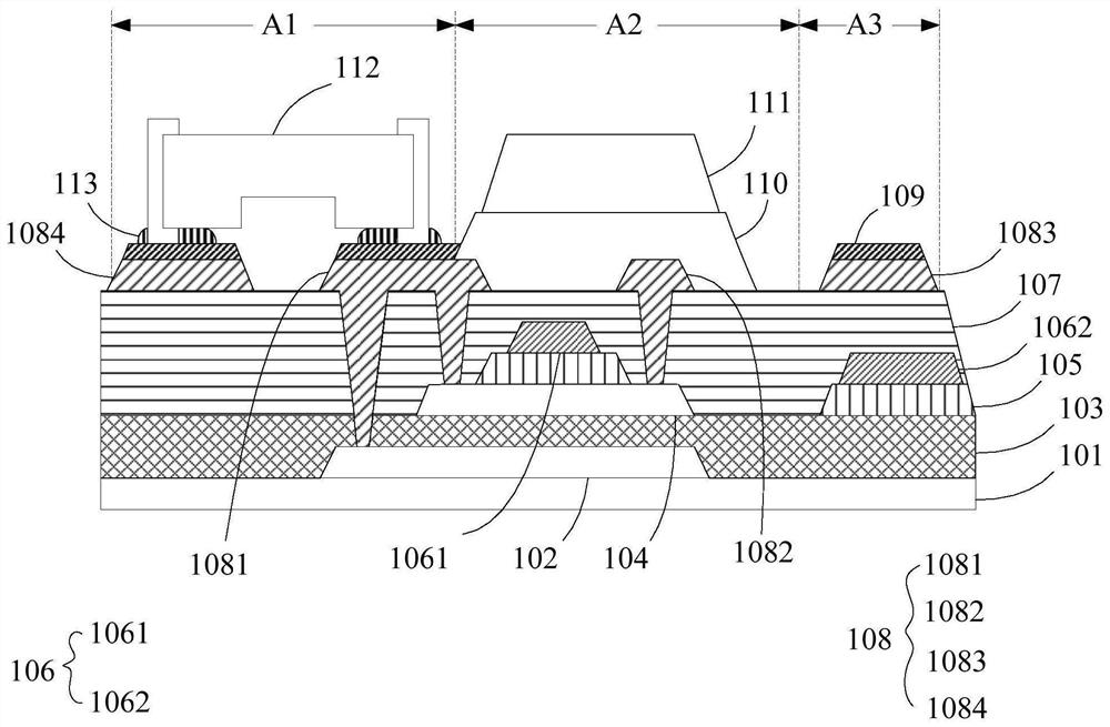
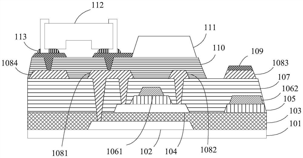
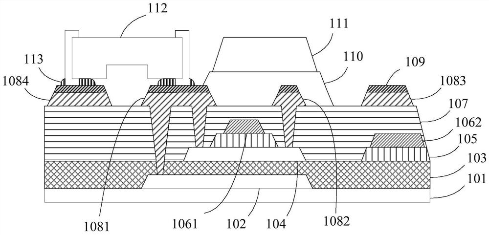
[0022] The following will clearly and completely describe the technical solutions in the embodiments of the present invention with reference to the drawings in the embodiments of the present invention. In the drawings, for clarity and ease of understanding and description, the size and thickness of the components shown in the drawings are not in scale.

[0023] Such as figure 1 As shown, it is a schematic diagram of the basic structure of the micro-light emitting diode display panel provided by the embodiment of the present invention. The substrate 101 , the first metal layer 106 , the interlayer insulating layer 107 and the second metal layer 108 .

[0024] In one embodiment, the micro-LED display panel further includes a light-shielding metal layer 102, a buffer layer 103, an active layer 104, a gate insulating layer 105, and an insulating layer 110, and the light-shielding metal layer 102 is located on the substrate On the substrate 101, it is used to shield the active la...


PUM


Abstract

The invention provides a micro light-emitting diode display panel, a preparation method thereof and a display device. The micro light-emitting diode display panel comprises a micro light-emitting diode binding area, a shading area and a peripheral wiring area, and the micro light-emitting diode display panel further comprises a substrate, a first metal layer located on the substrate, an interlayer insulating layer located on the first metal layer and a second metal layer located on the interlayer insulating layer. An anti-reflection layer used for reducing the reflectivity of the second metal layer is arranged on the second metal layer and corresponds to the micro light-emitting diode binding area and the peripheral wiring area. According to the anti-reflection layer provided by the invention, the reflection of the second metal layer to ambient light can be reduced, the contrast ratio of the micro light-emitting diode display panel is improved, and the display quality of the micro light-emitting diode display panel is improved.

Description

technical field [0001] The invention relates to the field of display technology, in particular to a micro-light-emitting diode display panel, a preparation method thereof, and a display device. Background technique [0002] MLED (Micro, Mini Light Emitting Diode, Micro Light Emitting Diode) is a new generation of display technology, which has higher brightness, better luminous efficiency and lower power consumption than the existing OLED (Organic Light Emitting Diode, Organic Light Emitting Diode) display technology. low, and thus received widespread attention. Large-sized micro-LED display panels are mainly formed by splicing multiple small-sized micro-light-emitting diode display panels, and multiple small-sized micro-light-emitting diode display panels are provided with a plurality of metal wiring pads in the peripheral wiring areas, so that large There are many splicing gaps in micro light-emitting diode display panels of small size. [0003] In addition, the micro-lig...

Claims


Application Information

Patent Timeline
IPC IPC(8): H01L33/44H01L33/62H01L33/58H01L25/075
CPCH01L33/44H01L33/62H01L33/58H01L25/0753H01L2933/0025H01L2933/0058H01L2933/0066
Inventor 卢马才
Owner SHENZHEN CHINA STAR OPTOELECTRONICS SEMICON DISPLAY TECH CO LTD
Features
  • Generate Ideas
  • Intellectual Property
  • Life Sciences
  • Materials
  • Tech Scout
  • Unparalleled Data Quality
  • Higher Quality Content
  • 60% Fewer Hallucinations
Learn More