Interface conversion circuit, chip, chip test system and method

An interface conversion and circuit technology, applied in the field of chip testing, can solve the problems of complex test vectors, long time required for chip testing, and low efficiency, so as to improve flexibility and efficiency, improve test efficiency, and reduce data transmission.

Pending Publication Date: 2021-06-22
上海燧原科技有限公司
View PDF0 Cites 0 Cited by
  • Summary
  • Abstract
  • Description
  • Claims
  • Application Information

AI Technical Summary

Problems solved by technology

With the high development of computing requirements, the software has higher and higher requirements for computing power, resulting in larger and larger chips and more complex

Method used


Image

  • Interface conversion circuit, chip, chip test system and method
  • Interface conversion circuit, chip, chip test system and method
  • Interface conversion circuit, chip, chip test system and method

Examples


Embodiment Construction

[0041] The present invention will be further described in detail below in conjunction with the accompanying drawings and embodiments. It should be understood that the specific embodiments described here are only used to explain the present invention, but not to limit the present invention. In addition, it should be noted that, for the convenience of description, only some structures related to the present invention are shown in the drawings but not all structures.

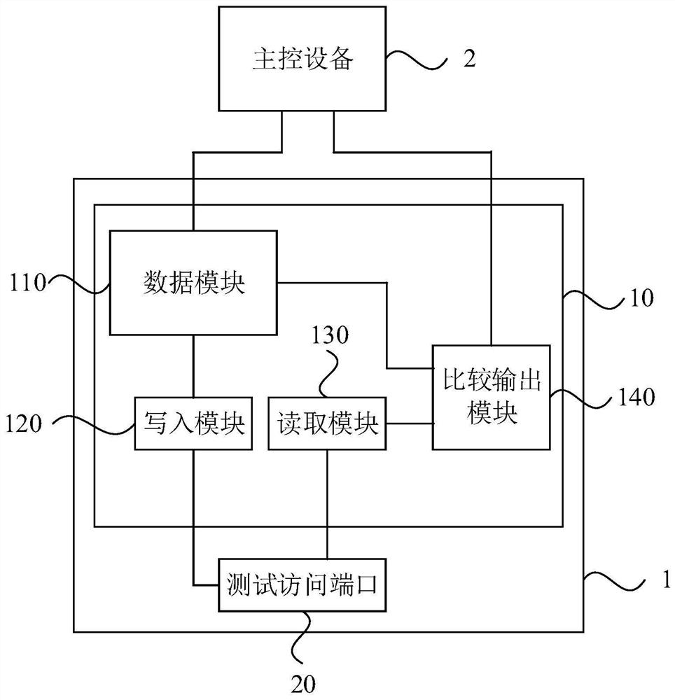
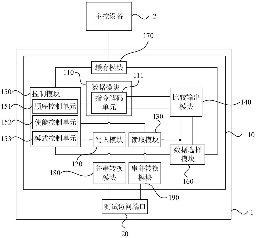
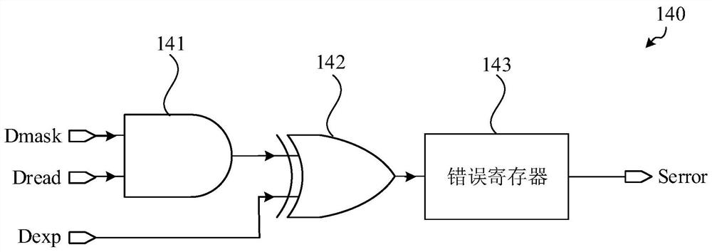
[0042] The embodiment of the present invention provides an interface conversion circuit, which is placed inside the chip under test and used for chip testing. figure 1 It is a schematic structural diagram of an interface conversion circuit provided by an embodiment of the present invention. see figure 1 , the interface conversion circuit 10 includes: a data module 110 , a write module 120 , a read module 130 and a comparison output module 140 .

[0043]Wherein, the interface conversion circuit 10 is placed in th...


PUM


Abstract

The invention discloses an interface conversion circuit, a chip, and a chip test system and method. The interface conversion circuit is arranged in the tested chip and comprises a data module, a write-in module, a read module and a comparison output module. The input end of the data module is connected with main control equipment; the data module is used for obtaining test excitation data and expected response data according to a test vector sent by the main control equipment; the input end of the write-in module is connected with the first output end of the data module, and the output end of the write-in module is connected with the input end of the test access port of the tested chip; the input end of the read module is connected with the output end of the test access port, and is used for collecting read data fed back by the tested chip; the first input end of the comparison output module is connected with the second output end of the data module, and the second input end is connected with the output end of the reading module; and the comparison output module is used for obtaining and outputting an error signal according to the read data and the expected response data. According to the embodiment of the invention, the flexibility and the efficiency of chip testing can be improved.

Description

technical field [0001] The embodiments of the present invention relate to the technical field of chip testing, and in particular to an interface conversion circuit, a chip, a chip testing system and a method. Background technique [0002] In order to ensure that the chip can work properly, the chip must be rigorously tested during and after the chip is manufactured. Usually, the chip test is carried out through the Joint Test Action Group (JTAG) test pin. The test method of the standard JTAG protocol is to pour test vectors into the chip at the test data input port, and then obtain the test vector at the test data output port. The response signal of the chip is used to detect whether the function of the chip is normal. The test circuit inside the chip is responsible for receiving and executing the test vector sent by the external test system, and then feedback the result vector to the external chip test system. With the high development of computing requirements, software ...

Claims


Application Information

Patent Timeline
IPC IPC(8): G01R31/28G01R1/04
CPCG01R1/0433G01R31/2863
Inventor 钱海涛
Owner 上海燧原科技有限公司
Why Eureka
Try Eureka