
Chip-level vacuum sealed electrostatic galvanometer

A vacuum-sealed, electrostatic technology, applied in the field of vibrating mirrors and electrostatic vibrating mirrors, can solve the problems of increased module volume, decreased packaging vacuum degree, and increased noise level, so as to expand the application field, reduce driving requirements, and reduce The effect of energy loss

Active Publication Date: 2021-06-22
XIAN CHISHINE OPTOELECTRONICS TECH CO LTD
View PDF4 Cites 2 Cited by
  • Summary
  • Abstract
  • Description
  • Claims
  • Application Information

AI Technical Summary

Problems solved by technology

This kind of noise has little impact on some applications, such as industrial 3D imaging, but in the field of consumer electronics, such noise seriously affects the user experience of the device. If the noise cannot be effectively eliminated, such a galvanometer cannot be truly scaled in consumer electronics. application
If vacuum packaging is used, it will increase the difficulty of sealing, increase the volume of the module, and increase the cost. At the same time, the current vacuum packaging of the vibrating mirror mainly uses adhesives and other methods, which are difficult to maintain the vacuum for a long time, and the package can be packaged in a short period of time. The vacuum degree drops, and the noise level rises significantly, and the galvanometer module cannot continue to be used in low-noise requirements scenarios

Method used


Image

  • Chip-level vacuum sealed electrostatic galvanometer
  • Chip-level vacuum sealed electrostatic galvanometer
  • Chip-level vacuum sealed electrostatic galvanometer

Examples


Embodiment Construction

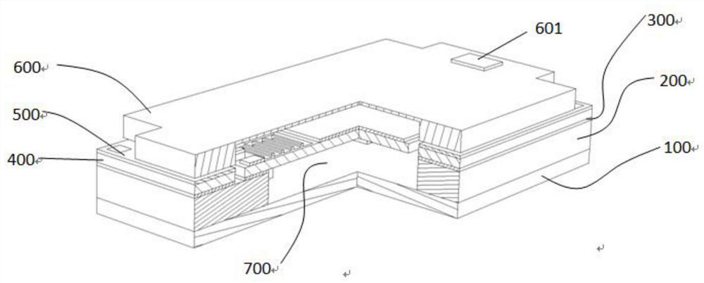
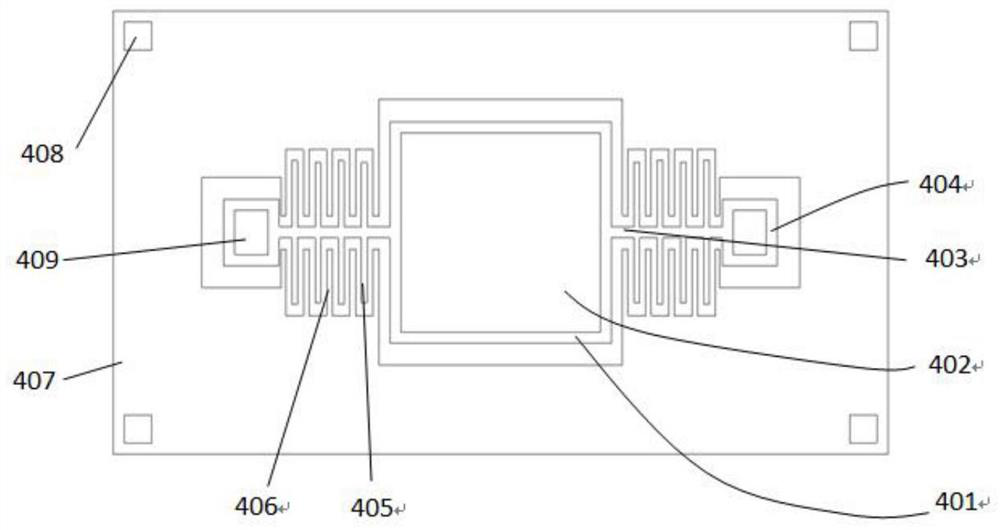
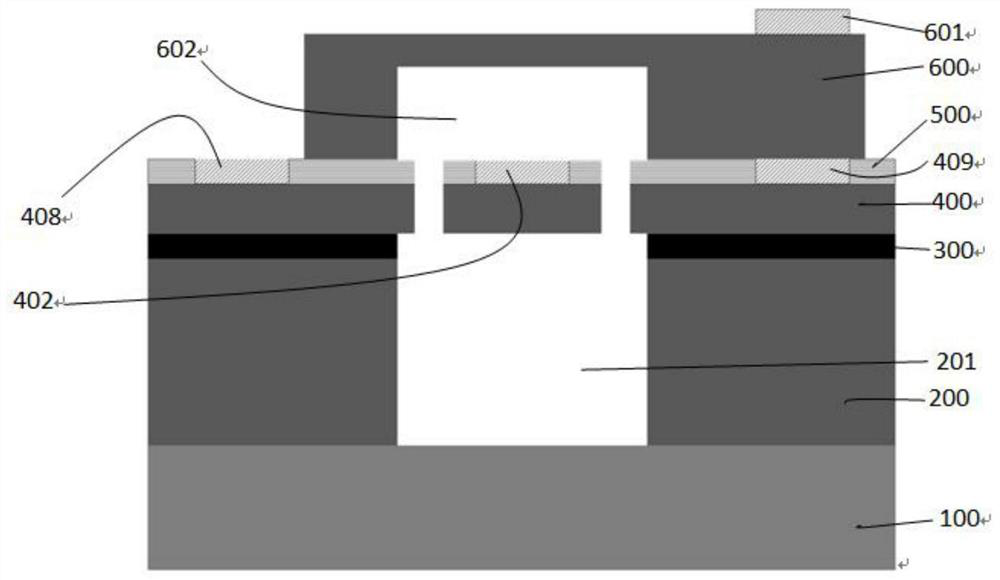
[0045] Such as figure 1 , 2 , a partial cross-sectional view of a vacuum-sealed single-axis galvanometer, which is composed of a substrate, a back cavity plate, an insulating layer, a structural layer, and a front cavity plate that are sequentially stacked and connected from bottom to top. The structural layer includes a mirror body, a mirror surface, a rotating shaft, an anchor body, a movable comb, a fixed comb, a pad and a fixed frame. The mirror surface is a thin layer of gold covering the upper surface of the mirror body, with a thickness of 100nm. The substrate, the back cavity plate, the insulating layer, the fixed frame of the structural layer and the front cavity plate are sequentially connected to form a closed cavity, and the reflector surface, reflector body, rotating shaft, anchor body, movable comb teeth and fixed comb teeth are all located in the closed cavity. inside the cavity.

[0046] Such as image 3 , the ground pad 409 communicates with the top pad 60...


PUM

PropertyMeasurementUnit
Thicknessaaaaaaaaaa
Thicknessaaaaaaaaaa
Thicknessaaaaaaaaaa

Abstract

The invention discloses a chip-level vacuum sealed electrostatic galvanometer which is formed by sequentially stacking and connecting a substrate, a back cavity plate, an insulating layer, a structural layer, a flat layer and a front cavity plate from bottom to top. The movable part of the galvanometer is located in a vacuum environment, compared with a galvanometer which is sealed in a non-vacuum mode, the movable part of the galvanometer does not act with air when vibrating, and therefore noise generated when the movable part acts with the air is eliminated. The energy of vibration in the movable structure material is extremely small, and due to the fact that the movable structure material is sealed in vacuum, a small amount of generated vibration cannot be conducted to the outside, and noise is further eliminated. When the galvanometer body, the driving comb teeth and other movable structures vibrate, no air damping exists, energy loss caused by the air damping is greatly reduced, and the power consumption of the galvanometer is remarkably reduced; when the galvanometer body, the driving comb teeth and other movable structures vibrate, no air damping exists, and a larger rotation angle can be obtained under the same driving voltage. And the required driving voltage is low at the same rotating angle, so that the application field of the galvanometer is further expanded, and the driving requirement is reduced.

Description

technical field [0001] The invention belongs to the field of optoelectronics, and relates to a vibrating mirror, in particular to a chip-level vacuum-sealed electrostatic vibrating mirror. Background technique [0002] Galvanometers based on MEMS technology are widely used in projection, 3D imaging, car navigation and other fields, and are one of the core devices in these fields. The current MEMS vibrating mirror itself is an open structure, that is, the reflective surface and movable structure of the vibrating mirror are exposed to the environment after the tape-out is completed, and the vibrating mirror is packaged in a sealed component through subsequent module packaging during use. In, to achieve the protection of the galvanometer. Most of the current galvanometer packages are non-vacuum packages, and the high-frequency vibration of the movable parts such as the mirror surface in the gas produces non-negligible noise during the work of the galvanometer. This kind of no...

Claims


Application Information

Patent Timeline
IPC IPC(8): G02B26/08
CPCG02B26/0841
Inventor 彭磊白民宇周少玮姜军委马力杨彪周翔杨涛王芳
Owner XIAN CHISHINE OPTOELECTRONICS TECH CO LTD
Learn More