

Periodic band domain structure analysis method of ferroelectric ceramic
A technology of ferroelectric ceramics and analysis methods, which is applied in instruments, scanning probe technology, scanning probe microscopy, etc. problem, to achieve the effect of large polarization value and good ferroelectricity
- Summary
- Abstract
- Description
- Claims
- Application Information
AI Technical Summary
Problems solved by technology
Method used
Image

Examples
Embodiment 1
[0044] Below, combine Figure 2-6 , describe this embodiment in detail.
[0045] (1) According to step S2, the phase characterization of ceramic samples, please refer to Figure 2-3 .
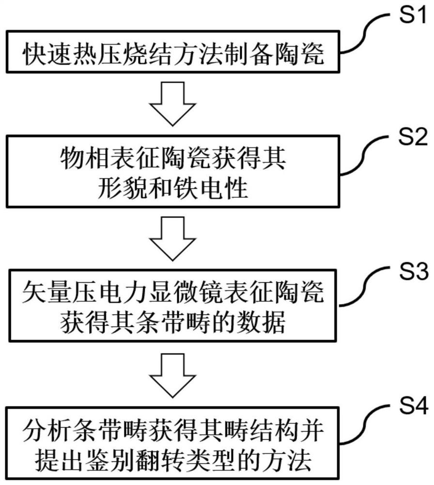
[0046] Generally, the ferroelectricity of thin films can be detected by ferroelectric loops, but if it is difficult to test ferroelectric loops in ultra-thin films or ceramic sheets, piezoelectric loops can be used to detect the local inversion characteristics and ferroelectric properties of the sample surface. The PFM needle tip is fixed at a point on the sample surface, and the piezoelectric signal is recorded while applying a DC bias voltage, and the applied voltage is in the range of -10V to +10V. In view of the fact that ceramics are polycrystalline samples with grain boundaries, we conduct tests in multiple regions and give two typical situations, see figure 2 .
[0047] figure 2 : PFM piezoelectric loop diagram of a ceramic sample. The PFM amplitude diagram above shows the magnit...
Embodiment 2
[0058] Below, combine Figure 7 , to illustrate this embodiment.
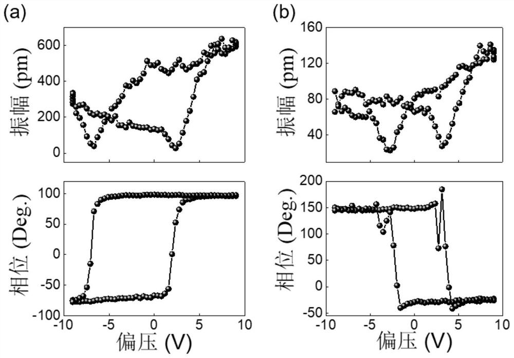
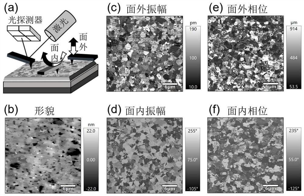
[0059] Figure 7 : (a-d) are vector PFM characterization results of 0° strip domain, which are out-of-plane PFM amplitude (a) and phase (b), in-plane PFM amplitude (c) and phase (d); (e-h) are ceramic samples The vector PFM characterization results of the stripe domain after rotating clockwise by 90°, which are out-of-plane PFM amplitude (e) and phase (f), in-plane PFM amplitude (g) and phase (h), respectively, and the image is rotated counterclockwise , which is convenient for comparative analysis with the 0° result. The morphology of the ceramic sample is given in (i), and it can be seen that the surface of the ceramic sample is smooth and flat. From the light-dark contrast in (b), it can be determined that the polarization has both upward and downward distributions, excluding the 71° domain, it may be a 109° or 180° domain, which can be determined from the light-dark contrast in (d) The polarization has ...
Embodiment 3
[0061] Below, combine Figure 8 , to illustrate this embodiment.
[0062] Figure 8 : (a-d) are vector PFM characterization results of 0° strip domain, which are out-of-plane PFM amplitude (a) and phase (b), in-plane PFM amplitude (c) and phase (d); (e-h) are ceramic samples The vector PFM characterization results of the stripe domain after rotating clockwise by 90°, which are out-of-plane PFM amplitude (e) and phase (f), in-plane PFM amplitude (g) and phase (h), respectively, and the image is rotated counterclockwise , which is convenient for comparative analysis with the 0° result. The morphology of the ceramic sample is given in (i), and it can be seen that the surface of the ceramic sample is smooth and flat. From the light-dark contrast in (b), it can be determined that the polarization has both upward and downward distributions, excluding the 71° domain, it may be a 109° or 180° domain, which can be determined from the light-dark contrast in (d) The polarization has ...
PUM
 Abstract
Description
Claims
Application Information