A Characterization Method of Periodic Stripe Domain Structure of Ferroelectric Thin Films

A ferroelectric thin film, periodic technology, applied in the direction of circuits, electrical components, electrical solid devices, etc., can solve the problem of not conducting more detailed analysis, etc., and achieve the effect of large polarization value and good ferroelectricity

Active Publication Date: 2021-10-29
HUAIYIN INSTITUTE OF TECHNOLOGY
View PDF7 Cites 0 Cited by
  • Summary
  • Abstract
  • Description
  • Claims
  • Application Information

AI Technical Summary

Problems solved by technology

In ferroelectric materials, the piezoelectric effect is a direct evidence of the existence of ferroelectric polarization; therefore, piezoelectric force microscopy (PFM) based on scanning probe microscopy (SPM) is an inseparable tool for studying polarization distribution at the nanoscale. Indispensable tool, the vector PFM characterization and analysis method developed from it can reorganize the three-dimensional polarization distribution of ferroelectric domains; for periodic strip domains, most of the relevant literatures currently give the Schematic diagram without a more detailed analysis

Method used


Image

  • A Characterization Method of Periodic Stripe Domain Structure of Ferroelectric Thin Films
  • A Characterization Method of Periodic Stripe Domain Structure of Ferroelectric Thin Films
  • A Characterization Method of Periodic Stripe Domain Structure of Ferroelectric Thin Films

Examples


Embodiment 1

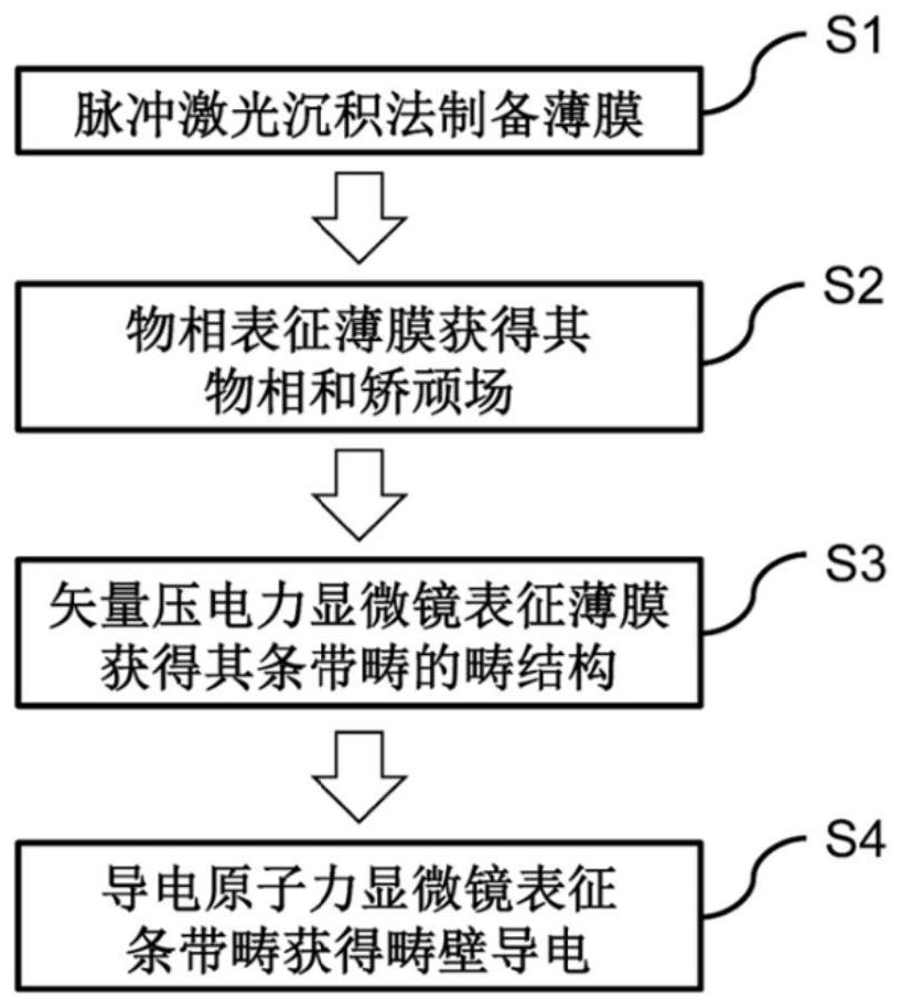
[0041] Such as Figure 1-8 as shown, figure 1 It is a schematic flowchart of a characterization method for a periodic striped domain structure of a ferroelectric thin film of the present invention. The operation and implementation parameters of using the PLD method to prepare the BFO thin film have been described in detail in the summary of the invention and the specific implementation manner. Combine below Figure 2-8 , describe this embodiment in detail.

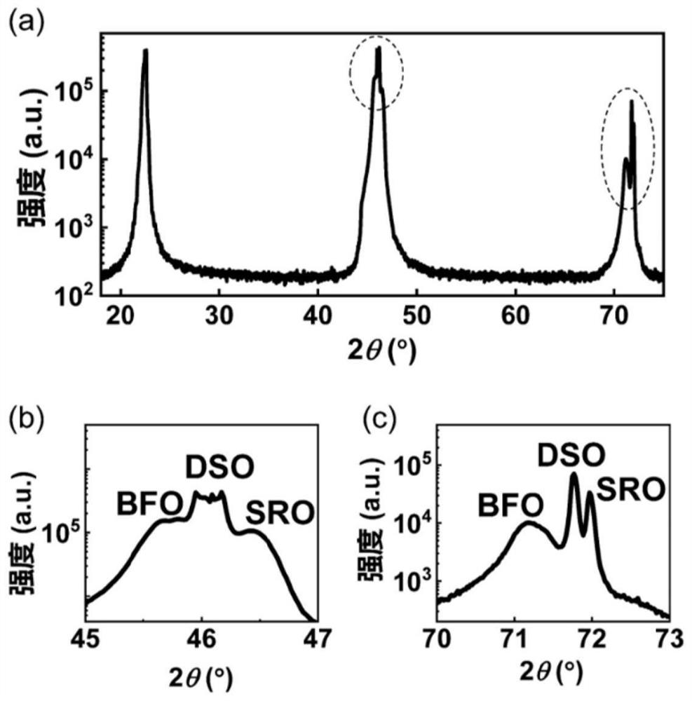
[0042] (1) According to step S2, phase characterization of film samples, please refer to Figure 2-4 .

[0043] figure 2 : X-ray θ-2θ scanning results of thin film samples, (a) is the result of wide range angle scanning, (b) is the enlarged view of 45°-47° range scanning results, where the DSO peak intensity exceeds the range, (c) is Enlarged view of the scanning results in the range of 70°-73°; one is to confirm the structure of the sample as DSO / SRO / BFO; The phase structure is close.

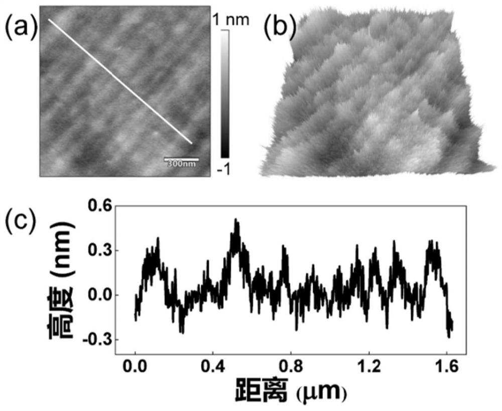
[0044] image 3 : AFM ima...


PUM

PropertyMeasurementUnit
thicknessaaaaaaaaaa
thicknessaaaaaaaaaa
surface roughnessaaaaaaaaaa

Abstract

The invention discloses a periodic striped domain structure of a ferroelectric thin film and a characterization method thereof, belonging to the technical field of micro-nano characterization, and the method comprises the following steps: preparing a bismuth ferrite thin film by pulse laser deposition; characterizing it by an X-ray diffractometer The lattice constant is determined to be a rhomboid phase structure, the piezoelectric butterfly curve is used to confirm its ferroelectricity and coercive voltage, and its morphology is characterized by atomic force microscopy; the periodic stripes in nanoferroelectric thin films are characterized by vector piezoelectric force microscopy Banded domains, the three-dimensional domain structure was determined by fine vector piezoelectric force microscopy analysis method; the domain walls of the striped domains were observed to conduct electricity by using conductive atomic force microscopy. The ferroelectric thin film preparation method provided by the present invention can be used in non-volatile, high-density ferroelectric random access memory; at the same time, the provided characterization method can accurately provide the three-dimensional domain structure and domain wall of the periodic strip domain Conduction; provide solutions for the development and characterization of high-density ferroelectric memory devices.

Description

technical field [0001] The invention relates to the technical field of micro-nano characterization, in particular to a characterization method for the periodic striped domain structure of a ferroelectric thin film. Background technique [0002] Ferroelectric random access memory has the advantages of low energy consumption, fast writing, and much larger erasing times, and is expected to become the next generation of non-volatile memory. Ferroelectric storage requires ferroelectric materials to have a large polarization value and strong piezoelectric response at room temperature, which is conducive to the development and detection of devices based on ferroelectric materials. Among them, bismuth ferrite (BiFeO 3 , abbreviated as BFO) the Curie temperature and Neel temperature of this material are 370 ° C and 830 ° C, respectively, with antiferromagnetic and ferroelectric properties, and the remanent polarization values ​​​​in the (111) and (001) directions are 100 μC / cm 2 ...

Claims


Application Information

Patent Timeline
Patent Type & Authority Patents(China)
IPC IPC(8): H01L27/11507
CPCH10B53/30
Inventor 翟俊杰李忠文南峰李冠男周舟黄煜焱
Owner HUAIYIN INSTITUTE OF TECHNOLOGY
Why Eureka
Try Eureka