

Semiconductor structure and manufacturing method thereof
A manufacturing method and semiconductor technology, applied in semiconductor/solid-state device manufacturing, electrical components, circuits, etc., to achieve the effects of avoiding adverse effects, improving production yield, and improving warpage changes
- Summary
- Abstract
- Description
- Claims
- Application Information
AI Technical Summary
Problems solved by technology
Method used
Image

Examples
Embodiment 1
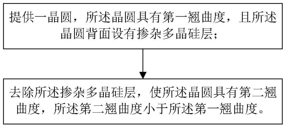
[0063] A method for fabricating a semiconductor structure is provided in this embodiment, please refer to figure 1 , shown as a process flow diagram of the method, comprising the following steps:
[0064] A wafer is provided, the wafer includes a front side for forming a semiconductor device and a back side relative to the front side, the wafer has a first degree of warpage, and a doped polysilicon layer is grown on the back side of the wafer;
[0065] The doped polysilicon layer is removed, so that the wafer has a second degree of warpage, and the second degree of warpage is smaller than the first degree of warpage.
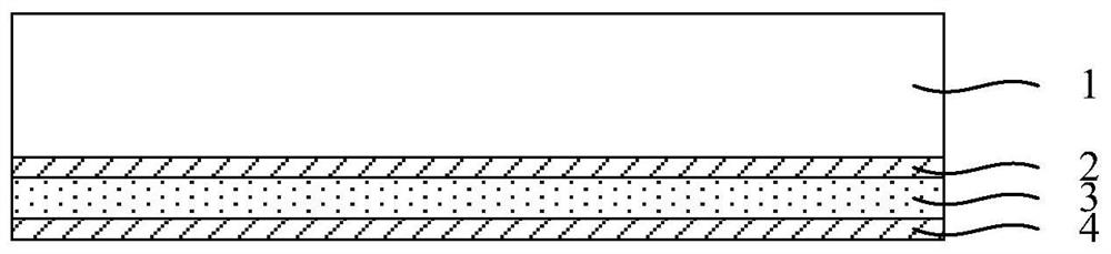
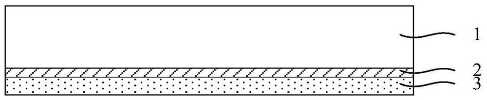
[0066] See first figure 2 , performing step S1: providing a wafer 1, the wafer 1 has a first degree of warpage, and the backside of the wafer 1 is provided with a doped polysilicon layer 3.
[0067] As an example, in the direction away from the back side of the wafer 1, the back side of the wafer 1 is provided with a first silicon dioxide layer 2, the doped p...
Embodiment 2
[0075] This embodiment adopts basically the same technical solution as Embodiment 1, the difference is that in this embodiment, after removing the doped polysilicon layer, a silicon dioxide layer is further formed on the back of the wafer, so that the wafer There is a third degree of warpage, the third degree of warpage being less than the second degree of warpage.
[0076] See first Figure 2 to Figure 4 , performing steps S1-S2 that are basically the same as those in Embodiment 1.
[0077] see again Figure 5 and Figure 6 , further forming a silicon dioxide layer on the back surface of the wafer 1 .
[0078] Specifically, since the chemical vapor phase method cannot form a silicon dioxide layer on the back of the wafer, in this embodiment, a furnace tube heating method is used to form a front silicon dioxide layer 5 and a back silicon dioxide layer 5 on the front and back sides of the wafer 1, respectively. Layer 6 (eg Figure 5 shown), and remove the front silicon dio...
Embodiment 3
[0083] In this embodiment, a semiconductor structure is provided, and the manufacturing method of the semiconductor structure as described in the first embodiment is adopted in the manufacturing process of the semiconductor structure.
PUM
| Property | Measurement | Unit |
|---|---|---|
| Thickness | aaaaa | aaaaa |
Abstract
Description
Claims
Application Information