BGA solder ball three-dimensional detection method based on depth image processing

A depth image, three-dimensional detection technology, applied in image data processing, image enhancement, image analysis and other directions, can solve the problem of high time-consuming processing methods and can not meet the requirements of real-time detection.

Pending Publication Date: 2021-06-29
XUZHOU NORMAL UNIVERSITY
View PDF0 Cites 3 Cited by
  • Summary
  • Abstract
  • Description
  • Claims
  • Application Information

AI Technical Summary

Problems solved by technology

Although the point cloud has the characteristics of high precision, it cannot meet the real-time detection requirements of the industry due to the high time-consuming processing method

Method used


Image

  • BGA solder ball three-dimensional detection method based on depth image processing
  • BGA solder ball three-dimensional detection method based on depth image processing
  • BGA solder ball three-dimensional detection method based on depth image processing

Examples


Embodiment 1

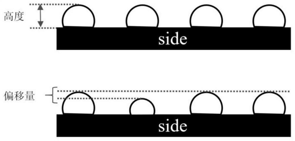
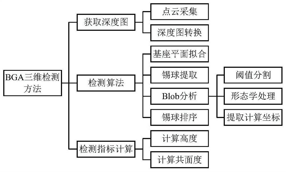
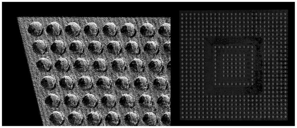
[0035] Such as figure 2 As shown, a BGA solder ball three-dimensional defect detection method based on depth image processing, first converts the collected chip point cloud into a depth image, fits the base plane of the chip and uses Blob analysis technology to mark each solder ball area, and then extracts the solder ball area. The 3D coordinate points corresponding to the 2D center point of the ball area and its 8 neighboring pixels are averaged and assigned to the 3D point on the top of the solder ball. In order to improve the robustness of the algorithm, when marking the solder ball area, the morphological method is combined to approximate the circular shape of the solder ball. Finally, calculate the distance from the vertex to the plane to obtain the solder ball height and coplanarity.

[0036]In this embodiment, the BGA chip point cloud data is obtained by a binocular 3D line-scanning camera modeled as Chromasens-3DPIXA, and displayed using the CloudCompare software pla...


PUM


Abstract

A BGA solder ball three-dimensional detection method based on depth image processing comprises the steps: converting a collected chip point cloud into a depth image, a base plane of a chip is fitted, and marking solder ball areas through a Blob analysis algorithm; extracting a two-dimensional central point of the solder ball region and three-dimensional coordinate points corresponding to eight neighborhood pixels of the solder ball region, performing averaging and assigning the average value to a three-dimensional point at the top of the solder ball; when the solder ball area is marked, combining with a morphological method to enable the solder ball to approach to circularity so as to improve the robustness of the algorithm; and finally calculating the distance from the vertex to the plane to obtain the height and coplanarity of the solder balls. According to the BGA solder ball three-dimensional detection method based on depth image processing, a machine vision technology is utilized, after depth image conversion is carried out on the collected chip point cloud by utilizing a point cloud and image processing technology, a solder ball three-dimensional detection index can be efficiently obtained, and the precision meets the detection requirement.

Description

technical field [0001] The invention relates to the technical fields of point cloud processing and image processing; in particular, it relates to a BGA solder ball three-dimensional defect detection method based on depth image processing. Background technique [0002] As domestic and foreign companies continue to develop the chip industry chain in China, chip packaging and testing technology has developed rapidly. The Ball Grid Array (BGA) chip is one of many integrated chips, and the packaging quality of the ball-planting process directly affects the performance and reliability of the chip. The small diameter of the solder ball and the high precision of the detection index make the ordinary contact measurement technology unable to meet the requirements. The detection technologies currently applied to BGA chips mainly include: solder ball detection based on X-rays, solder ball detection based on planar image processing technology, and solder ball surface defect detection ba...

Claims


Application Information

Patent Timeline
Patent Type & Authority Applications(China)
IPC IPC(8): G06T7/00G06T7/136G06T5/30
CPCG06T5/30G06T7/0004G06T2207/10028G06T2207/20036G06T2207/30148G06T7/136G06T7/73
Inventor 梁天为朱呈祥陈浩
Owner XUZHOU NORMAL UNIVERSITY
Why Eureka
Try Eureka