
LED chip assembly, manufacturing method thereof, LED device and manufacturing method of LED device

A technology of LED chips and LED devices, which is applied in the direction of electric solid-state devices, semiconductor devices, electrical components, etc., can solve the problems of high light energy and uneven luminous color, achieve uniform luminous color, uniform light color, and omit the packaging process Effect

Pending Publication Date: 2021-06-29
SHENZHEN JUFEI OPTOELECTRONICS CO LTD
View PDF0 Cites 1 Cited by
  • Summary
  • Abstract
  • Description
  • Claims
  • Application Information

AI Technical Summary

Problems solved by technology

[0003] The present invention provides an LED chip assembly, an LED device and a manufacturing method thereof, which solves the problem that the light energy in the normal direction of the existing LED chip is much higher than the light energy in the four sides, resulting in uneven luminous color.

Method used


Image

  • LED chip assembly, manufacturing method thereof, LED device and manufacturing method of LED device
  • LED chip assembly, manufacturing method thereof, LED device and manufacturing method of LED device
  • LED chip assembly, manufacturing method thereof, LED device and manufacturing method of LED device

Examples


Embodiment Construction

[0053] In order to make the object, technical solution and advantages of the present invention clearer, the embodiments of the present invention will be further described in detail below through specific implementation manners in conjunction with the accompanying drawings. It should be understood that the specific embodiments described here are only used to explain the present invention, not to limit the present invention.

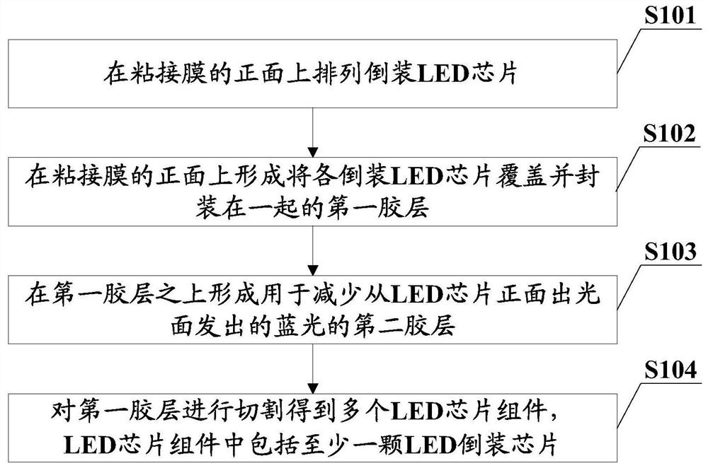
[0054] This embodiment provides a method for manufacturing an LED chip assembly. The front light-emitting surface of the flip-chip LED chip included in the manufactured LED chip assembly is at least partially covered with a second adhesive layer for reducing light energy, thereby reducing the size of the flip-chip LED chip. The difference between the light energy in the normal direction of the chip and the light energy on the four sides improves the uniformity of the luminous color.

[0055] For ease of understanding, this embodiment is combined below fig...


PUM


Abstract

The invention provides an LED chip assembly, a manufacturing method thereof, an LED device and a manufacturing method of the LED device. Inverted LED chips are arranged on the front face of a bonding film, and the positive electrode and the negative electrode of each LED inverted chip are bonded to the front face of the bonding film; a first adhesive layer is formed on the front surface of the adhesive film, wherein the first adhesive layer is used for covering and packaging the flip LED chips together; a second adhesive layer used for reducing light energy emitted from the light-emitting surfaces of the front faces of the LED chips is formed on the first adhesive layer, and the second adhesive layer at least partially covers the light-emitting surfaces of the front faces of the flip LED chips and does not cover the first adhesive layer between the adjacent LED chips; and the first adhesive layer is cut to obtain a plurality of LED chip assemblies. The second adhesive layer used for reducing light energy is formed on the front surface of each LED flip chip, so that the difference between the light energy in the forward normal direction of the flip LED chips and the light energy of the four side surfaces can be reduced, and the uniformity of light emitting colors is improved.

Description

technical field [0001] The present invention relates to the field of LED (Light Emitting Diode, light emitting diode), in particular to an LED chip assembly, an LED device and a manufacturing method thereof. Background technique [0002] Video quality directly affects people's emotions and quality of life, and ultra-high-definition video 8K is the future development direction. Mini LED and Micro LED can be used as backlight or direct display, which complies with the development requirements of ultra-high-definition video. Whether it is backlight (blue light or white light) or direct display (RGB), uniform light emission and consistent color are required. At present, Mini LED is used as the first method of backlight: place and fix flip-chip blue light chips with a certain distance on the substrate, mold a layer of transparent adhesive layer, pass in current to drive the blue light chip to emit blue light, and the blue light excites the QD film (quantum dots) film) and then ...

Claims


Application Information

Patent Timeline
Patent Type & Authority Applications(China)
IPC IPC(8): H01L25/16H01L25/00H01L33/56H01L33/58
CPCH01L25/167H01L25/50H01L33/56H01L33/58
Inventor 孙平如苏宏波
Owner SHENZHEN JUFEI OPTOELECTRONICS CO LTD
Learn More