Supercharge Your Innovation With Domain-Expert AI Agents!

Optoelectronic semiconductor device with substrate structure

An optoelectronic semiconductor and substrate structure technology, applied in the direction of semiconductor devices, electrical components, circuits, etc., can solve the problems of affecting the stability of pins, difficult to radiate temperature, and damage to other devices, so as to facilitate replacement and maintenance, avoid Tin-plated fixation, the effect of prolonging the service life

Active Publication Date: 2021-06-29
HENAN UNIV OF URBAN CONSTR
View PDF11 Cites 0 Cited by
  • Summary
  • Abstract
  • Description
  • Claims
  • Application Information

AI Technical Summary

Problems solved by technology

[0003] However, the existing optoelectronic semiconductor devices with a carrier film and a substrate structure have some shortcomings during use. Generally, pins are used to fix them. When the pins are under too much force, they are easy to cause damage and affect the pins. The stability of the connection, the chip is also soldered to the circuit board by soldering the pins, which causes the bottom of the chip to be in full contact with the circuit board, and the device will be damaged when it is used. After the damage, it needs to be soldered to the lead The tin on the pin is liquefied to take out the device, but this process will cause damage to other connected devices; secondly, the temperature generated when the chip is working is difficult to dissipate, and it is easy to cause damage to the device when the internal heat cannot be dissipated for a long time. The damage will affect its service life. Therefore, an optoelectronic semiconductor device with a substrate structure is proposed

Method used


Image

  • Optoelectronic semiconductor device with substrate structure
  • Optoelectronic semiconductor device with substrate structure
  • Optoelectronic semiconductor device with substrate structure

Examples


Embodiment Construction

[0026] The following will clearly and completely describe the technical solutions in the embodiments of the present invention with reference to the accompanying drawings in the embodiments of the present invention. Obviously, the described embodiments are only some, not all, embodiments of the present invention.

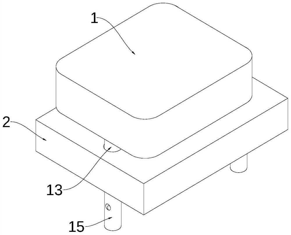
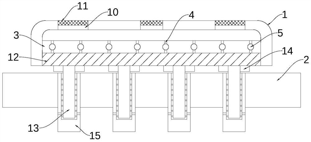
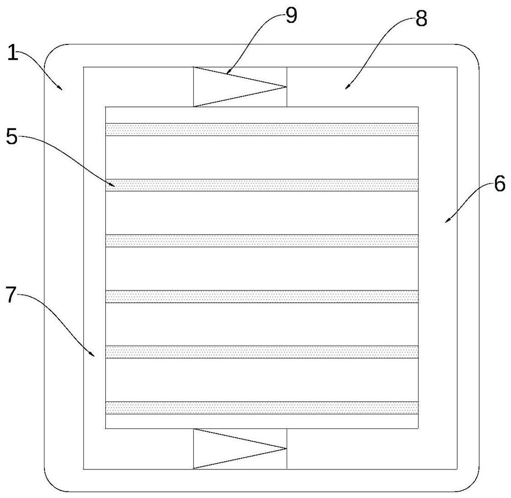
[0027] refer to Figure 1-6 , an optoelectronic semiconductor device with a substrate structure, including a device body and a substrate 2, a connection mechanism is provided on the substrate 2, the device body includes a housing 1, a heat conduction device and a locking mechanism, and the device body is located above the substrate 2 ;

[0028] The heat conduction device includes a heat conduction mechanism and a heat dissipation mechanism. The heat conduction mechanism includes a heat dissipation plate 3, a collecting pipe 7, and a drive chamber 6. The outer wall of the heat dissipation plate 3 is fixedly connected with the inner wall of the housing 1. There are ca...


PUM


Abstract

The invention discloses an optoelectronic semiconductor device with a substrate structure. The optoelectronic semiconductor device comprises a device body and a substrate, wherein a connecting mechanism is arranged on the substrate, the device body comprises a shell, a heat conduction device and a clamping mechanism, the device body is located above the substrate, the heat conduction device comprises a heat conduction mechanism and a heat dissipation mechanism, the heat dissipation mechanism comprises a plurality of air outlets formed in the top part of the shell, the inner side walls of the air outlets are fixedly connected with dustproof nets, the clamping mechanism comprises a conductive plate fixedly connected to the inner side wall of the shell, the bottom part of the conductive plate is fixedly connected with pins, and the connecting mechanism comprises a plurality of insertion blocks fixedly connected to the substrate. According to the optoelectronic semiconductor device, current flows and is conducted to the electric vibration sheet, the vibration of the electric vibration sheet periodically extrudes and stretches the driving cavity, cooling liquid flows and is collected into the collecting pipe, heat in the device is rapidly conducted to the outside, the device is prevented from being damaged due to too high temperature during use, and the service life of the device is effectively prolonged.

Description

technical field [0001] The invention relates to the field of electronic devices, in particular to an optoelectronic semiconductor device with a substrate structure. Background technique [0002] Optoelectronic semiconductor devices refer to various functional devices made using semiconductor photo-electronic (or electro-photon) conversion effects, which are different from semiconductor optical devices (such as optical waveguide switches, optical modulators, optical deflectors, etc.), optical devices The design principle is based on the change of the propagation mode of guided wave light by the external field. It is also different from the optoelectronic devices used by early people. The latter only focuses on the reception and conversion of light energy (such as photoresistors, photocells, etc.). Early optoelectronic devices were limited to For passive applications, the advent of semiconductor lasers as a coherent optical carrier source in the 1960s brought it into the stage...

Claims


Application Information

Patent Timeline
Patent Type & Authority Applications(China)
IPC IPC(8): H01L31/0203H01L31/024H01L33/62H01L33/64
CPCH01L31/0203H01L31/024H01L33/62H01L33/647
Inventor 王新刚侯宁贺伟王丹阳赵红梅庞凯歌刘晓芳张洛花陈英胡玥
Owner HENAN UNIV OF URBAN CONSTR
Features
  • R&D
  • Intellectual Property
  • Life Sciences
  • Materials
  • Tech Scout
  • Unparalleled Data Quality
  • Higher Quality Content
  • 60% Fewer Hallucinations
Learn More