Electrostatic discharge protection circuit

A technology for electrostatic discharge protection and circuits, which is applied to circuits, electrical components, electric solid devices, etc., and can solve problems such as damage to the gate oxide layer

Inactive Publication Date: 2003-12-10
LG SEMICON CO LTD
View PDF0 Cites 0 Cited by
  • Summary
  • Abstract
  • Description
  • Claims
  • Application Information

AI Technical Summary

Problems solved by technology

Therefore, when the trigger voltage of the ESD protection circuit is greater than the breakdown voltage of the gate oxide layer,

Method used


Image

  • Electrostatic discharge protection circuit
  • Electrostatic discharge protection circuit
  • Electrostatic discharge protection circuit

Examples


Embodiment Construction

[0028] Preferred embodiments of the present invention will be described in detail below with examples shown in the accompanying drawings.

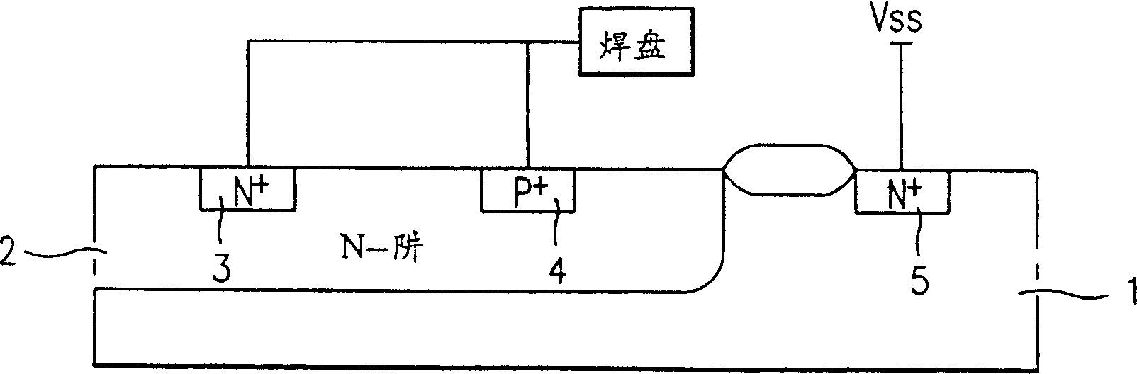
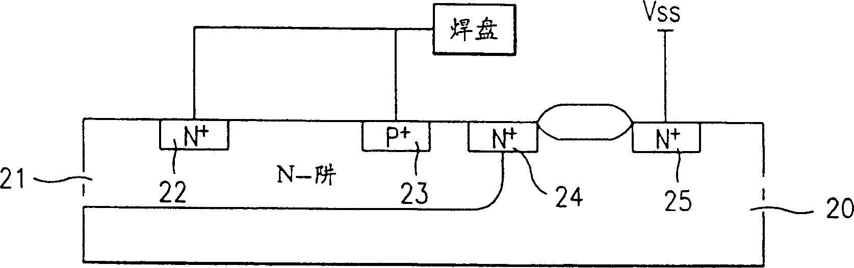
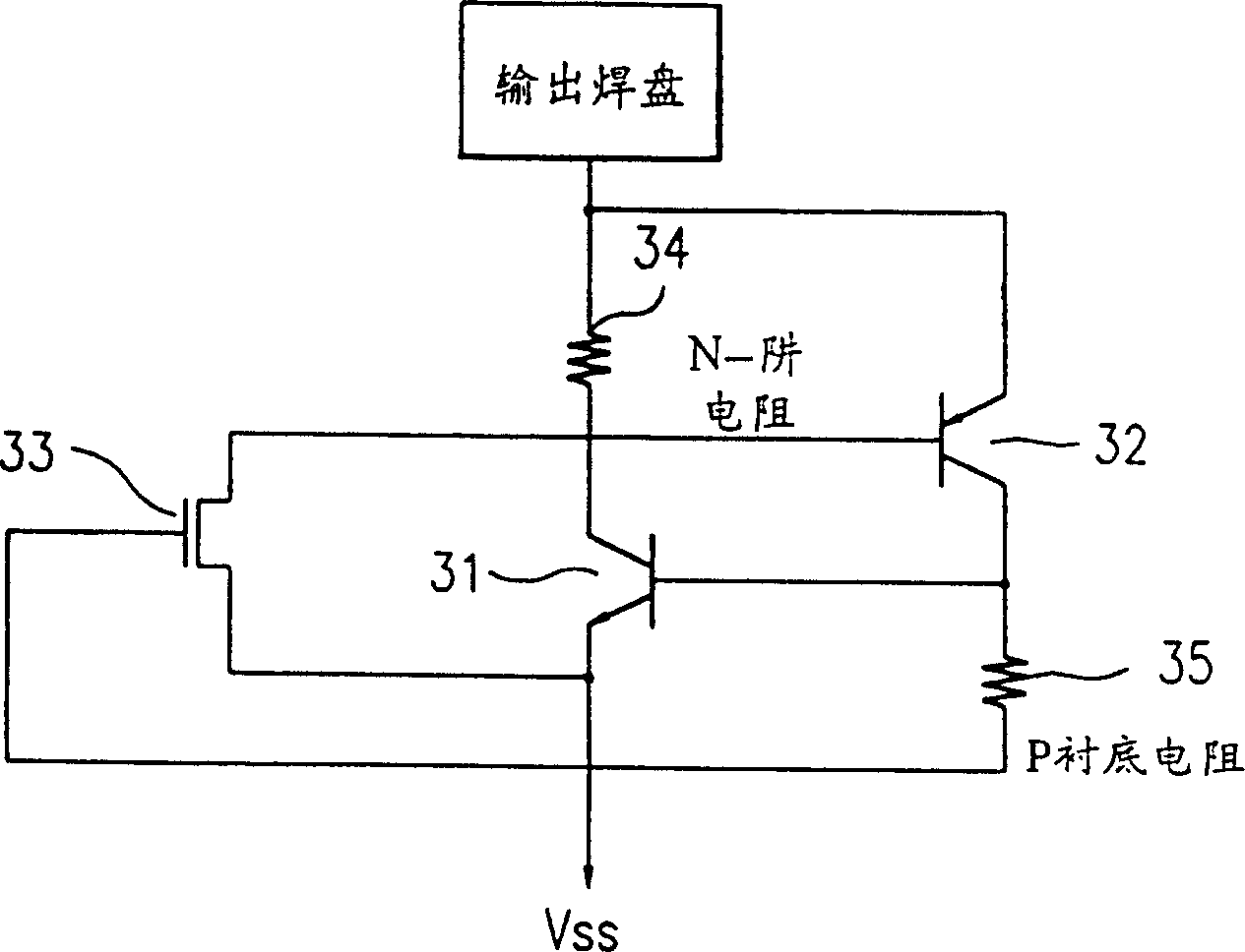
[0029] Figure 4A Represent the circuit configuration of the control gate SCR ESD protection circuit according to the present invention, Figure 4B is a cross-sectional view of a control gate SCR ESD protection circuit according to the present invention. see Figure 4A, the control gate SCR circuit includes: a first transistor 41 whose collector is connected to the output pad, the emitter of the first transistor 41 is connected to the Vss line; a second transistor 42 whose collector is connected to the base of the first transistor 41 , the emitter of the second transistor 42 is connected to the output pad; its source is connected to the MOS transistor 43 of the base of the second transistor 42, the drain of the MOS transistor 43 is connected to the emitter of the first transistor 41, the MOS transistor 43 The control gate is connected t...


PUM


Abstract

The ESD protection circuit disclosed, including: a second conductivity of well formed in a predetermined portion of a first conductivity of semiconductor substrate; a first conductivity of first impurity region and second conductivity of second impurity region, formed in the second conductivity of well; a first gate electrode formed on the semiconductor substrate, and second gate electrode formed on the first gate electrode, the first gate electrode being isolated from the semiconductor substrate; second conductivity of third and fourth impurity regions, formed in a portion of the semiconductor substrate, the portion being placed on both sides of the first and second gate electrodes; and a second conductivity of fifth impurity region formed on the semiconductor substrate, the fourth and fifth impurity regions having an isolation layer therebetween.

Description

technical field [0001] The invention relates to an electrostatic discharge (ESD) protection circuit, in particular to an ESD protection circuit, which can reduce the trigger voltage of a silicon controlled rectifier (SCR) and improve its performance. Background technique [0002] Conductive or oxide layers of semiconductor devices can be thermally damaged by ESD. In order to reduce the device breakdown caused by ESD, the main method is to remove the ESD inducement around the device, and another method is to use a suitable ESD protection circuit for continuous discharge without affecting the internal circuit of the device. Meanwhile, an SCR used as an ESD protection circuit has high efficiency in current-voltage characteristics, but its trigger voltage is high. [0003] A conventional ESD protection circuit will be described below with reference to the accompanying drawings. figure 1 is a cross-sectional view of a conventional lateral silicon controlled rectifier (LSCR) for...

Claims


Application Information

Patent Timeline
IPC IPC(8): H01L29/74H01L27/02H01L27/06H01L29/749
CPCH01L29/7436H01L27/0251H01L27/0262H01L29/87H01L2924/0002H01L2924/00H01L27/06
Inventor 郑爀采
Owner LG SEMICON CO LTD
Why Eureka
Try Eureka