Flip heat source chip and preparation method and application method thereof

A technology of chip and heat source, which is applied in the field of flip-chip heat source chip and its preparation, to achieve the effect of improving heat dissipation capacity, temperature uniformity and accurate measurement results

Active Publication Date: 2021-07-09
SOUTHWEST CHINA RES INST OF ELECTRONICS EQUIP
View PDF10 Cites 0 Cited by
  • Summary
  • Abstract
  • Description
  • Claims
  • Application Information

AI Technical Summary

Problems solved by technology

[0007] However, there are still few reports on how to construct a flip-chip heat source chip to realize real-time and in-situ measurement of chip temperature while generating heat, so as to accurately analyze the heat dissipation capability of flip-chip-based electronic systems.

Method used


Image

  • Flip heat source chip and preparation method and application method thereof
  • Flip heat source chip and preparation method and application method thereof
  • Flip heat source chip and preparation method and application method thereof

Examples


Embodiment 1

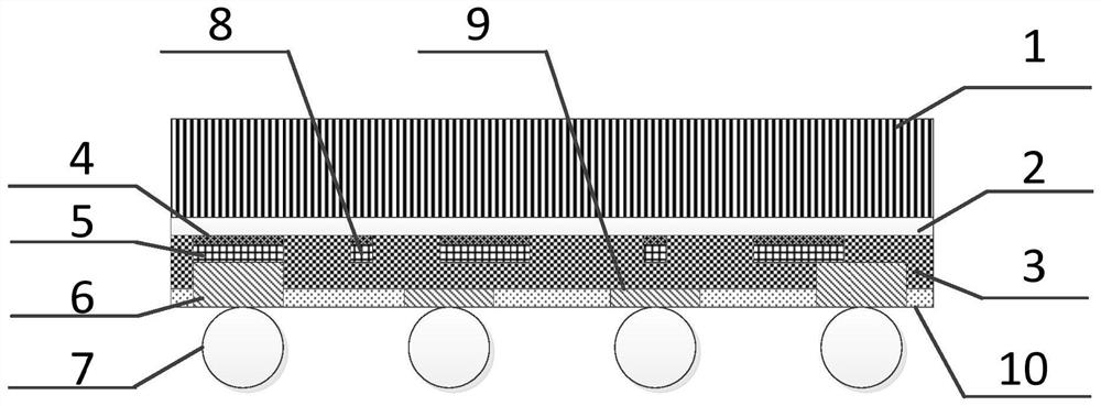
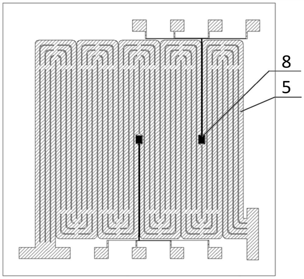
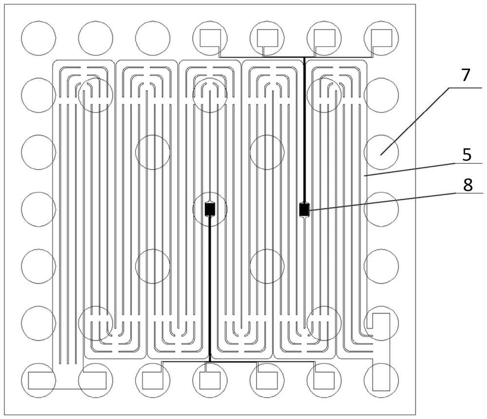
[0052] This embodiment provides a flip-chip heat source chip, such as figure 1 As shown, it includes: chip substrate 1, bottom insulating layer 2, heat conduction passivation layer 3, solder resist layer 10, adhesion layer 4, heating resistor 5, temperature sensor 8, metal interconnection pad 6, metal heat conduction pad 9 and micro-bumps 7, wherein the chip substrate 1, the bottom insulating layer 2, the heat conduction passivation layer 3 and the solder resist layer 10 are sequentially connected. A heating resistor 5 and a plurality of temperature sensors 8 are arranged in the thermally conductive passivation layer 3 , and the heating resistor 5 and the temperature sensors 8 are connected to the bottom insulating layer 2 through an adhesive layer 4 . A plurality of metal interconnection pads 6 and a plurality of metal heat conduction pads 9 are penetratingly arranged in the solder resist layer 10, the metal interconnection pads 6 are electrically connected to the heating res...

Embodiment 2

[0058] On the basis of Embodiment 1, this embodiment provides a flip-chip heat source chip, wherein: the chip substrate 1 is Si with a thickness of 300 μm; the bottom insulating layer 2 is SiO x Insulating film with a thickness of 300nm; the thermal conduction passivation layer 3 is SiN x Insulating film with a thickness of 400nm; the adhesion layer 4 is a Ti film with a thickness of 10nm; the heating resistor 5 and the temperature sensor 8 are W (tungsten) thin films with a thickness of 300nm, and the resistance of the heating resistor 5 is 20 ohms. The resistance of 8 is 2000 ohms; the metal interconnection pad 6 and the metal heat conduction pad 9 are Ti / Au metal pads; the solder resist layer 10 is SiN x The insulating film has a thickness of 100nm; the micro bumps 7 are gold bumps.

Embodiment 3

[0060] On the basis of Example 1, this embodiment provides a method for preparing a flip-chip heat source chip, such as Figure 6 shown, including the following steps:

[0061] Step 101: providing a chip substrate 1;

[0062] Step 102: growing a bottom insulating layer 2 on the surface of the chip substrate 1 using thin film vapor deposition technology;

[0063] Step 103: Prepare an adhesion layer 4 on the surface of the bottom insulating layer 2 by magnetron sputtering;

[0064] Step 104: Prepare a temperature-resistant thin film metal on the surface of the adhesion layer 4 by using thin film vapor deposition technology;

[0065] Step 105: using photolithography combined with thin film etching technology to prepare heat-resistant thin film metal into heating resistor 5 and temperature sensor 8;

[0066] Step 106: Prepare a thermally conductive passivation layer 3 on the surface of the heating resistor 5 and the temperature sensor 8 using thin film vapor deposition technolo...


PUM

PropertyMeasurementUnit
thicknessaaaaaaaaaa
thicknessaaaaaaaaaa
thicknessaaaaaaaaaa

Abstract

The invention discloses a flip heat source chip and a preparation method and application method thereof, and the flip heat source chip comprises a chip substrate, a bottom insulating layer, a heat conduction passivation layer, a solder mask layer, an adhesion layer, a heating resistor, a temperature sensor, a metal interconnection bonding pad, a metal heat conduction bonding pad, and a micro bump. The chip substrate, the bottom insulating layer, the heat-conducting passivation layer and the solder mask layer are connected in sequence; a heating resistor and a plurality of temperature sensors are arranged in the heat conduction passivation layer, and the heating resistor and the temperature sensors are connected with the bottom insulation layer through an adhesion layer; a plurality of metal interconnection bonding pads and a plurality of metal heat conduction bonding pads are arranged in the solder mask in a penetrating manner, the metal interconnection bonding pads are electrically connected with the heating resistor and the temperature sensor, the metal heat conduction bonding pads are connected with the heat conduction passivation layer, and micro convex points are arranged on the surfaces of the metal interconnection bonding pads and the metal heat conduction bonding pads. The chip can simulate heating of a real flip chip, and can measure the temperature of the flip chip in real time and in situ, thereby accurately analyzing the heat dissipation capability of an electronic system based on the flip chip.

Description

technical field [0001] The invention relates to the technical field of microelectronic heat dissipation, in particular to a flip-chip heat source chip, a preparation method and an application method thereof. Background technique [0002] With the development of microelectronics technology, the volume and integration density of electronic systems are gradually increasing. Traditional front-mount chips rely on metal leads to achieve electrical interconnection with the outside; since the lead interconnection pads are usually located outside the chip, it takes up a larger integration area, which limits the further improvement of the integration density of electronic systems based on front-mount chips. Flip chip achieves electrical interconnection with the outside by flipping the chip and preparing micro-bumps on its surface; since the interconnection pad of the micro-bump is usually located at the bottom of the chip, it does not occupy an additional integration area and can achi...

Claims


Application Information

Patent Timeline
Patent Type & Authority Applications(China)
IPC IPC(8): H01L25/18H01L23/367H01L23/31H01L21/56
CPCH01L25/18H01L23/3672H01L23/3128H01L21/563
Inventor 张剑卢茜向伟玮曾策董乐赵明叶惠婕蒋苗苗朱晨俊叶永贵
Owner SOUTHWEST CHINA RES INST OF ELECTRONICS EQUIP
Why Eureka
Try Eureka