Display panel and preparation method thereof

A technology for display panels and substrates, applied in electrical components, electrical solid devices, circuits, etc., can solve problems such as metal layer step difference, and achieve the effects of reducing step difference, increasing flatness, and large thickness

Inactive Publication Date: 2021-07-09
SHENZHEN CHINA STAR OPTOELECTRONICS SEMICON DISPLAY TECH CO LTD
View PDF3 Cites 2 Cited by
  • Summary
  • Abstract
  • Description
  • Claims
  • Application Information

AI Technical Summary

Problems solved by technology

[0003] The embodiment of the present application provides a display panel and its preparation method, which solves the step difference problem caused by the patterning of the metal layer in the prior art without increasing the process.

Method used


Image

  • Display panel and preparation method thereof
  • Display panel and preparation method thereof
  • Display panel and preparation method thereof

Examples


Embodiment Construction

[0029] The technical solutions in the embodiments of the present application will be clearly and completely described below in conjunction with the accompanying drawings in the embodiments of the present application. Obviously, the described embodiments are only some of the embodiments of the present application, not all of them. Based on the embodiments in this application, all other embodiments obtained by those skilled in the art without making creative efforts belong to the scope of protection of this application.

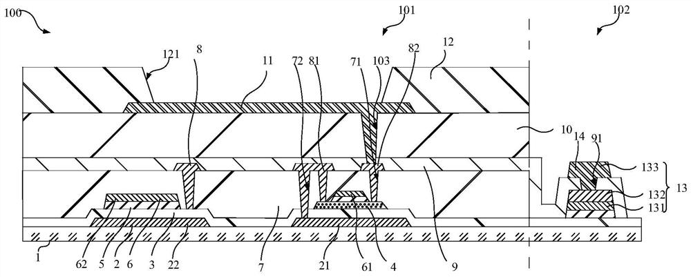
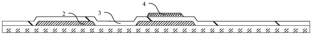
[0030] The present application provides a display panel, including a substrate, a thin film transistor and a first flat layer. The thin film transistor is arranged on the substrate. A thin film transistor includes a gate, a source, and a drain. The first flat layer is disposed between the gate and the source. The first flat layer is an organic insulating layer. In this application, the first flat layer is set between the gate, the source and the drain of the...


PUM


Abstract

Embodiments of the invention disclose a display panel and a preparation method thereof. The display panel comprises a substrate and a thin film transistor arranged on the substrate, wherein the thin film transistor comprises a grid electrode, a source electrode and a drain electrode. The display panel further comprises a first flat layer arranged between the grid electrode and the source electrode, wherein the first flat layer is an organic insulating layer. According to the display panel, the first flat layer is arranged between the grid electrode and the source and drain electrodes of the thin film transistor, the first flat layer is made of an organic insulating material and has large thickness and good filling and leveling performance, and the flatness of the surface of the display panel can be improved under the condition that a manufacturing process and a panel structure do not need to be additionally increased.

Description

technical field [0001] The present application relates to the field of display technology, in particular to a display panel and a manufacturing method thereof. Background technique [0002] As the resolution, aperture ratio, and refresh rate of display panels continue to increase, the influence of signal line resistance on the display performance of the display panel becomes more and more obvious. In order to ensure the display performance, the thickness of the signal line is also increasing, resulting in a large step difference on the surface of the structure above the signal line, which affects the progress of the subsequent manufacturing process. Contents of the invention [0003] Embodiments of the present application provide a display panel and a manufacturing method thereof, which solve the level difference problem caused by patterning the metal layer in the prior art without increasing the manufacturing process. [0004] An embodiment of the present application pro...

Claims


Application Information

Patent Timeline
Patent Type & Authority Applications(China)
IPC IPC(8): H01L27/32H01L27/15
CPCH01L27/156H10K59/124H10K59/12H10K59/1201
Inventor 张乐陶徐梦达
Owner SHENZHEN CHINA STAR OPTOELECTRONICS SEMICON DISPLAY TECH CO LTD
Why Eureka
Try Eureka