Filter Power Divider Based on Integrated Substrate Gap Waveguide
A gap waveguide and integrated substrate technology, applied in the electronic field, can solve the problems of narrow bandwidth of filter power splitter and unsuitable high-frequency band, etc., and achieve the effect of high isolation and wide bandwidth
- Summary
- Abstract
- Description
- Claims
- Application Information
AI Technical Summary
Problems solved by technology
Method used
Image

Examples
Embodiment 1
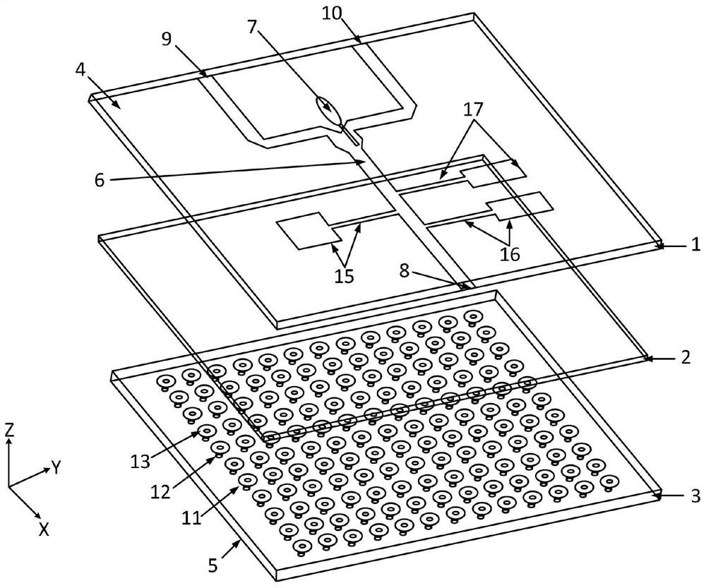
[0064] In Embodiment 1 of the present invention, as Figure 1 to Figure 6 As shown, the filter power divider based on the integrated substrate gap waveguide includes an electromagnetic bandgap structure for shielding electromagnetic radiation energy, a filter power divider structure for energy transmission, an upper dielectric board 1, a lower dielectric board 3, and upper and lower dielectric boards. The middle layer dielectric board 2 that acts as a spacer between the layer dielectric boards, the electromagnetic bandgap structure is located on the lower dielectric board 3, and the gap 7 designed to add isolation resistance is located on the first metal layer 4 on the upper surface of the upper dielectric board 1, The structure of the filtering power dividing circuit is formed by cascading the filtering circuit and the power dividing circuit, and the total microstrip line 6 formed by the circuit is located on the lower surface of the upper dielectric board 1 . The filtering c...
Embodiment 2
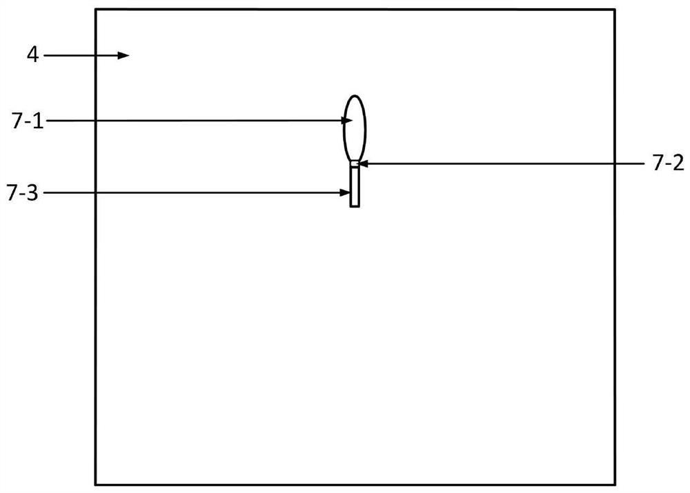
[0073] Such as Figure 7 to Figure 10 As shown, the filter power divider based on the integrated substrate gap waveguide of the second embodiment has similar technical characteristics to the filter power divider based on the integrated substrate gap waveguide of the first embodiment, and the same thing is that the filtering of the two The power dividing circuits are the same in structure and size; the difference is that the shape of the gap 7 of the first metal layer 4 on the upper surface of the upper dielectric board 1 is different. The slit 7 of the filter power divider based on the integrated substrate gap waveguide of embodiment one is composed of an elliptical slit 7-1 and a rectangular slit 7-3, and the slit of the filter power divider based on the integrated substrate gap waveguide of embodiment two 7 consists of two rectangular slots 7-1 and 7-3.
[0074] The filter power divider based on the integrated substrate gap waveguide of this embodiment has the following cha...
Embodiment 3
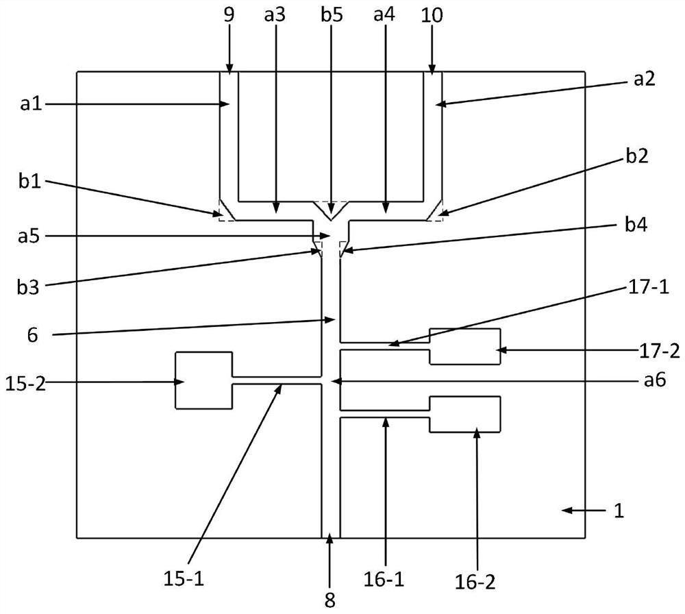
[0078] Such as Figure 11 to Figure 16 As shown, the filter power divider based on the integrated substrate gap waveguide in the third embodiment has the same technical characteristics as the filter power divider based on the integrated substrate gap waveguide in the first embodiment, the difference is that the branch The three ladder impedances connected on both sides of the microstrip line a6 transform the ratio of the electrical length of the microstrip line to the ladder impedance, that is, the first branch and the second branch (15-1, 15-2, 16-1, 16 -2, 17-1, 17-2) have a smaller size than the filter power splitter based on the integrated substrate gap waveguide in the first embodiment.
[0079] The filter power divider based on the integrated substrate gap waveguide of this embodiment has the following characteristics in practical applications:
[0080] According to actual application requirements, the electrical lengths of the first branch and the second branch (15-1, ...
PUM
 Abstract
Description
Claims
Application Information
 - R&D
- Intellectual Property
- Life Sciences
- Materials
- Tech Scout
- Unparalleled Data Quality
- Higher Quality Content
- 60% Fewer Hallucinations
Browse by: Latest US Patents, China's latest patents, Technical Efficacy Thesaurus, Application Domain, Technology Topic, Popular Technical Reports.
© 2025 PatSnap. All rights reserved.Legal|Privacy policy|Modern Slavery Act Transparency Statement|Sitemap|About US| Contact US: help@patsnap.com