Method and structure for measuring photoetching overlay error before and after epitaxy

A photolithography overlay and error technology, applied in semiconductor/solid-state device testing/measurement, optics, and patterned surface photoengraving process, etc., can solve the problem of inability to accurately measure the offset before and after epitaxy, and eliminate expansion blur. , the effect of precise lithography overlay error

Active Publication Date: 2021-07-13
SHANGHAI SILIGHT TECH
View PDF16 Cites 1 Cited by
  • Summary
  • Abstract
  • Description
  • Claims
  • Application Information

AI Technical Summary

Problems solved by technology

[0005] The purpose of the present invention is to provide a method and structure for measuring the overlay error before and after epitax

Method used


Image

  • Method and structure for measuring photoetching overlay error before and after epitaxy
  • Method and structure for measuring photoetching overlay error before and after epitaxy
  • Method and structure for measuring photoetching overlay error before and after epitaxy

Examples


Embodiment Construction

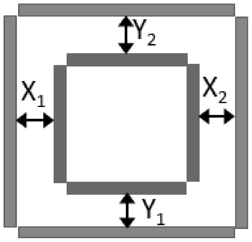
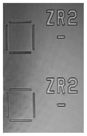
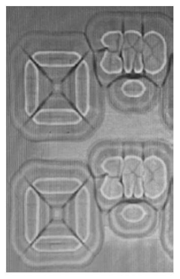
[0033] The method and structure for measuring the overlay error before and after epitaxy proposed by the present invention will be further described in detail below in conjunction with the accompanying drawings and specific embodiments. Advantages and features of the present invention will be apparent from the following description and claims. It should be noted that all the drawings are in a very simplified form and use imprecise scales, and are only used to facilitate and clearly assist the purpose of illustrating the embodiments of the present invention.

[0034] In addition, unless otherwise stated, features in different embodiments of the present invention can be combined with each other. For example, a feature in the second embodiment may be used to replace a corresponding or functionally identical or similar feature in the first embodiment, and the resulting embodiment also falls within the scope of disclosure or description of the present application.

[0035] The cor...


PUM


Abstract

The invention provides a method and structure for measuring photoetching overlay errors before and after epitaxy, and the method comprises the steps: carrying out the etching on the surface of a first substrate, and forming a vernier main scale original mark; carrying out epitaxy on the first substrate surface to form a second substrate surface, setting a vernier main ruler scale mark according to the existing morphology of the vernier main ruler scale original mark, and setting the original point of the vernier main ruler scale mark; carrying out photoetching on the surface of the second substrate to form vernier scale marks; and detecting the actual alignment point of the vernier main scale scale mark and the vernier scale scale mark, and calculating the photoetching overlay error according to the actual alignment point and the vernier scale precision.

Description

technical field [0001] The invention relates to the technical field of integrated circuits, in particular to a method and structure for measuring photolithography overlay errors before and after epitaxy. Background technique [0002] Epitaxial growth is a very critical process in the design of semiconductor devices, such as one of the key factors for the device to achieve complex charge balance, but in actual processes, epitaxial growth may make each semiconductor device defined by photolithography and etching processes Distortion of part geometry or expansion obscuring alignment measurement marks defined on the substrate surface prior to epitaxy. [0003] Identify by overlay error measuring equipment such as figure 1 The monitoring structure shown. The large frame and the small frame are formed by different photoresist layers. By measuring the distance difference between the two borders of the large frame and the small frame in the X direction, the offset in the X direct...

Claims


Application Information

Patent Timeline
IPC IPC(8): G03F9/00H01L21/66H01L23/544
CPCG03F9/7088G03F9/708H01L22/12H01L22/20H01L22/30
Inventor 李冰李营营
Owner SHANGHAI SILIGHT TECH
Why Eureka
Try Eureka