On-chip measurement method and system for electromagnetic immunity of SRAM

An electromagnetic immunity and on-chip measurement technology, applied in static memory, instruments, etc., can solve the problem of not being able to accurately obtain the interference range of the internal power supply pad, SRAM read and write separately, and achieve the effect of occupying a small chip area

Active Publication Date: 2021-07-13
SUN YAT SEN UNIV
View PDF7 Cites 0 Cited by
  • Summary
  • Abstract
  • Description
  • Claims
  • Application Information

AI Technical Summary

Problems solved by technology

[0011] The primary purpose of the present invention is to provide an on-chip measurement method of SRAM electromagnetic immunity, which solves the problem that the existing SRAM electromagnetic interference test method cannot accurately obtain the interference amplitude of the internal power supply Pad and the separate measurement of SRAM read and write

Method used


Image

  • On-chip measurement method and system for electromagnetic immunity of SRAM
  • On-chip measurement method and system for electromagnetic immunity of SRAM
  • On-chip measurement method and system for electromagnetic immunity of SRAM

Examples


Embodiment 1

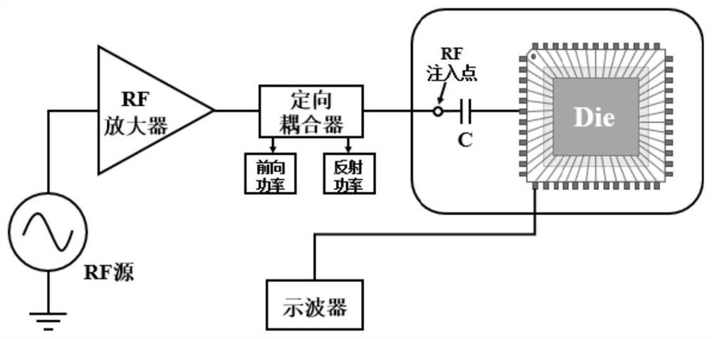
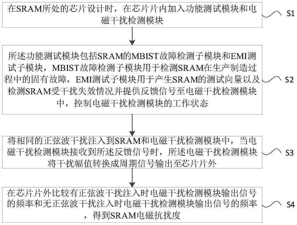
[0051] This embodiment provides an on-chip measurement method of SRAM electromagnetic immunity, such as image 3 , including the following steps:

[0052] S1: When designing the chip where the SRAM is located, add a functional test module and an electromagnetic interference detection module to the chip;

[0053] S2: The functional test module includes a MBIST fault detection sub-module and an EMI test sub-module, the MBIST fault detection sub-module is used to detect inherent faults in the SRAM manufacturing process, and the EMI test sub-module is used to generate SRAM test vectors and detect The SRAM is disturbed and fails and provides a feedback signal to the electromagnetic interference detection module to control the working state of the electromagnetic interference detection module;

[0054] S3: Inject the same sine wave interference into the SRAM and the electromagnetic interference detection module. When the electromagnetic interference detection module receives the fe...

Embodiment 2

[0073] This embodiment provides an on-chip measurement system of SRAM electromagnetic immunity, including:

[0074] Described function test module comprises MBIST failure detection submodule and EMI test submodule, and MBIST failure detection submodule is used for detecting the inherent failure of SRAM in the manufacturing process, and EMI test submodule is used for generating the test vector of SRAM and detecting SRAM affected Interference failure and provide feedback signals to the electromagnetic interference detection module to control the working status of the electromagnetic interference detection module

[0075] A power supply interference detection module, the power supply interference detection module is arranged in the chip, and the same sine wave interference is injected into the SRAM and the electromagnetic interference detection module. When the electromagnetic interference detection module receives the feedback signal, the electromagnetic interference detection mo...


PUM


Abstract

The invention discloses an on-chip measurement method and system for electromagnetic immunity of an SRAM. An interference amplitude of an internal power supply Pad is converted into a periodic signal by utilizing the characteristic that the periodicity of a signal of an electromagnetic interference detection module is not influenced by packaging, and the power supply voltage interference amplitude ARFI can be represented by detecting the frequency of the signal. And test vectors of read and write operations of the SRAM can be generated through the function test module, and the disturbed failure condition of the SRAM can be judged. A feedback signal is mainly further provided to control the on-off state of the ring oscillator, the power consumption of the ring oscillator is reduced, reading or writing in different working states of the SRAM is separated for immunity testing, and mutual influence is avoided.

Description

technical field [0001] The invention relates to the field of integrated circuit testing, in particular to an on-chip measurement method and system for SRAM electromagnetic immunity. Background technique [0002] The test standard IEC 62132 is mainly used for the immunity test of integrated circuits from 150KHz to 1GHz. It is divided into two test methods: radiation immunity and conduction immunity. Among them, the direct power injection method is the more commonly used immunity test method. [0003] The current DPI (direct power injection) test method for the immunity of integrated circuit chips is as follows: figure 1 Shown: The failure criterion is obtained according to the function of the chip, electromagnetic interference is injected on the VDD pin of the chip power supply, the signal related to the test is observed with an oscilloscope, and the electromagnetic immunity is characterized by using the forward injected power. [0004] Digital storage oscilloscopes have pow...

Claims


Application Information

Patent Timeline
IPC IPC(8): G11C29/12G11C29/56G11C29/50
CPCG11C29/12G11C29/56G11C29/50Y02D10/00
Inventor 粟涛徐小清张志文
Owner SUN YAT SEN UNIV
Why Eureka
Try Eureka