
Photoresist coating device and photoresist coating method

A coating device and photoresist technology, applied in optics, opto-mechanical equipment, photo-engraving process coating equipment, etc., can solve problems such as insufficient effect, cleaning agent sputtering, etc., and achieve the effect of improving process yield

Pending Publication Date: 2021-07-20
XIA TAI XIN SEMICON QING DAO LTD
View PDF0 Cites 0 Cited by
  • Summary
  • Abstract
  • Description
  • Claims
  • Application Information

AI Technical Summary

Problems solved by technology

However, the effect of removing the photoresist in this way is not sufficient, and it is possible to sputter the cleaning agent onto the photoresist at the non-edge of the wafer

Method used


Image

  • Photoresist coating device and photoresist coating method
  • Photoresist coating device and photoresist coating method
  • Photoresist coating device and photoresist coating method

Examples


Embodiment Construction

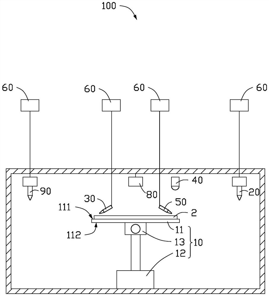
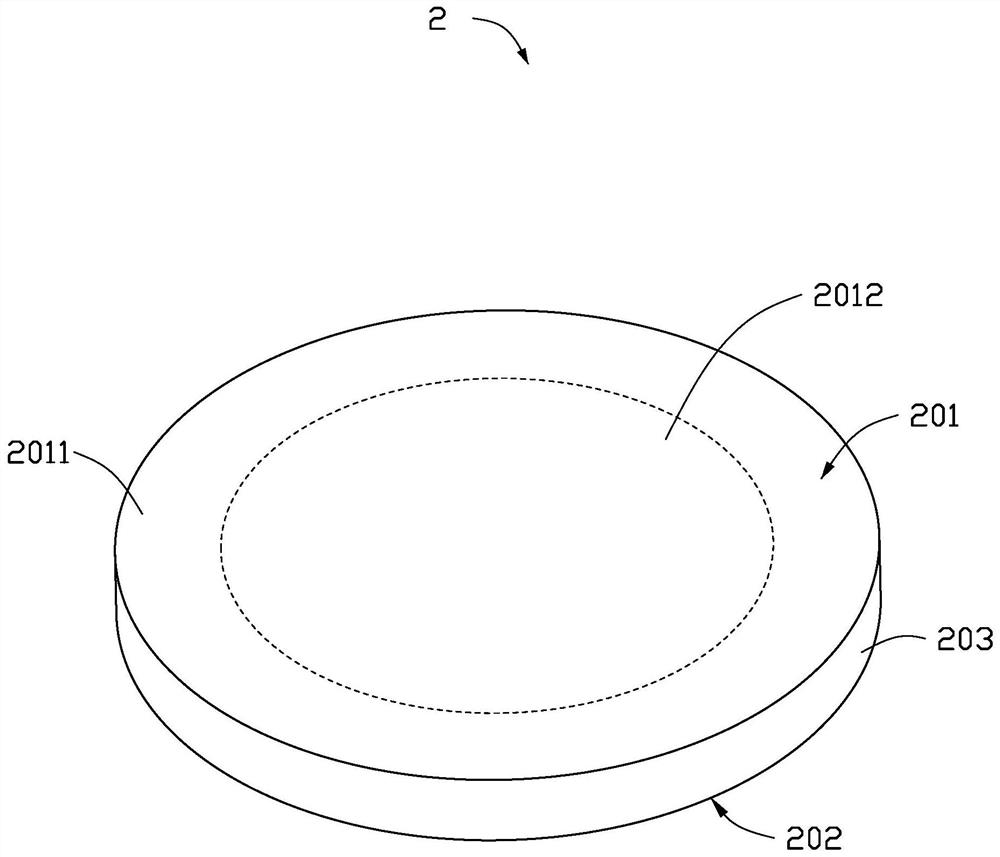
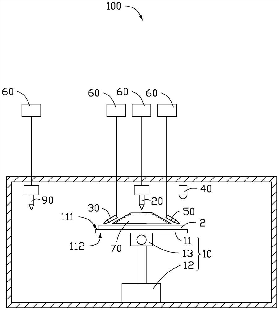
[0040] The following will clearly and completely describe the technical solutions in the embodiments of the present invention with reference to the accompanying drawings in the embodiments of the present invention. Obviously, the described embodiments are only some of the embodiments of the present invention, not all of them. Based on the embodiments of the present invention, all other embodiments obtained by persons of ordinary skill in the art without making creative efforts belong to the protection scope of the present invention.

[0041] It should be noted that when an element or component is considered to be “connected” to another element or component, it may be directly connected to the other element or component or there may be an intervening element or component at the same time. When an element or component is referred to as being "disposed on" another element or component, it can be directly disposed on the other element or component or intervening elements or compone...


PUM


Abstract

A photoresist coating device comprises a chuck, a photoresist nozzle, a cleaning agent nozzle, an edge exposure light source, a developing agent nozzle and an adjusting mechanism, wherein the chuck positions a wafer and drives the wafer to rotate, the photoresist nozzle sprays photoresist to the wafer positioned on the chuck, the cleaning agent nozzle sprays a cleaning agent to the photoresist on the edge of the wafer, the edge exposure light source exposes photoresist on the edge of the wafer, the developing agent nozzle sprays a developer to the photoresist on the edge of the exposed wafer, and the adjusting mechanism adjusts the cleaning agent nozzle to keep the angle between the sprayed cleaning agent and the surface of the wafer smaller than 30 degrees. The adjusting mechanism adjusts the developing agent nozzle to keep the angle between the sprayed developing agent and the surface of the wafer smaller than 30 degrees. According to the photoresist coating device provided by the invention, the photoresist can be fully removed, the cleaning agent is prevented from being sputtered to the photoresist at the non-edge of the wafer, and the photoetching yield is improved. The invention also provides a photoresist coating method.

Description

technical field [0001] The invention relates to the field of semiconductor processing, in particular to a photoresist coating device and a photoresist coating method. Background technique [0002] Integrated circuits are usually made by photolithography, which typically uses a light source to transfer the pattern on the mask to the photoresist on the surface of the wafer. In the photolithography process, photoresist is spin-coated on the wafer surface. The composition of photoresist generally includes photosensitive resin, sensitizer and solvent. During spin coating, the photoresist is dispersed from the center of the wafer to the edge of the wafer due to the centrifugal force of rotation, and most of the solvent has evaporated when the photoresist reaches the edge of the wafer. Also, the relative airflow at the edge of the wafer is greater, causing the solvent to evaporate faster than the center of the wafer. After the solvent is reduced, the viscosity of the photoresist...

Claims


Application Information

Patent Timeline
IPC IPC(8): G03F7/16
CPCG03F7/162
Inventor 田笵焕林钟吉张成根金在植
Owner XIA TAI XIN SEMICON QING DAO LTD
Learn More