Wafer transfer method and wafer transfer platform

A wafer transfer box and wafer technology, applied in the direction of transportation and packaging, electrical components, conveyor objects, etc., can solve problems such as cross influence, wafer pollution, wafer yield impact, etc., to ensure pollution and improve costs Low, to avoid the effect of cross-effect

Inactive Publication Date: 2021-07-20
璞芯半导体科技(苏州)有限公司 +1
View PDF22 Cites 2 Cited by
  • Summary
  • Abstract
  • Description
  • Claims
  • Application Information

AI Technical Summary

Problems solved by technology

[0003] When the wafer is produced and processed, it needs to go through a multi-step process, and the wafer needs to be transported through multiple channels during the process; at present, the existing wafer is directly returned to the front after the process is processed in the process chamber. In the open FOUP, the processed wafers are mixed with the unprocessed wafers in the FOUP, which may cause cross-effects between the two, making the processed wafers Contaminated, which has a great impact on the yield of the wafer

Method used


Image

  • Wafer transfer method and wafer transfer platform
  • Wafer transfer method and wafer transfer platform

Examples


Embodiment Construction

[0028] The present invention will be further described in detail below in conjunction with the accompanying drawings and specific embodiments.

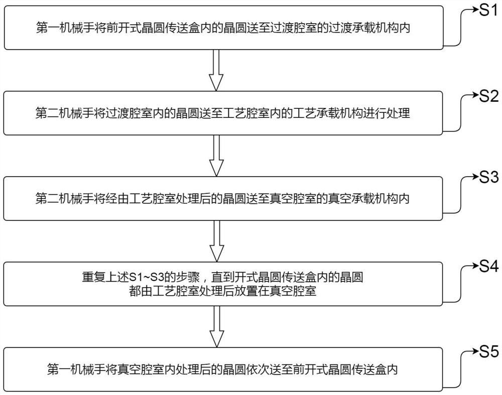
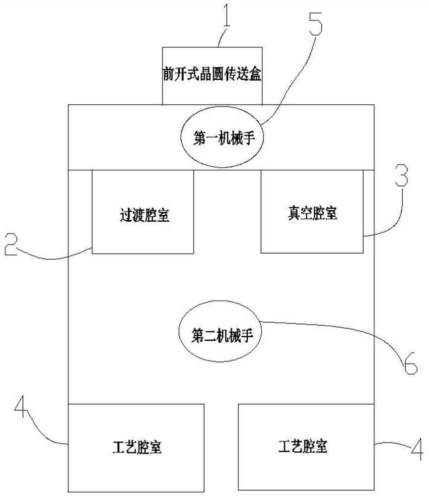
[0029] Please refer to the attached figure 2 , a wafer transfer platform according to an embodiment of the present invention includes a front-opening wafer transfer box 1, a transition chamber 2, a vacuum chamber 3, a process chamber 4, a first manipulator 5 and a second Manipulator 6; the front-opening FOUP 1 is used for loading wafers. In this embodiment, twenty-five wafers are placed in the FOUP 1 as a whole.

[0030] One side of the front-opening wafer transfer box 1 is provided with a transition chamber 2 and a vacuum chamber 3; wherein, the transition chamber 2 is provided with a transition carrying mechanism (not shown in the figure) for carrying wafers ); said vacuum chamber 3 is provided with a vacuum carrying mechanism (not shown) for carrying wafers, and said vacuum carrying mechanism is provided with twenty-five card slo...


PUM


Abstract

The invention discloses a wafer transfer method and a wafer transfer platform. The wafer transfer method comprises the following steps: S1, a first manipulator conveys a wafer in a front open type wafer conveying box into a transition bearing mechanism of a transition chamber; S2, a second manipulator sends the wafer in the transition chamber to a process bearing mechanism in the process chamber for processing; s3, the second manipulator sends the wafer processed by the process chamber into a vacuum bearing mechanism of the vacuum chamber; s4, the steps from S1 to S3 are repeated until the wafers in the open wafer transfer box are all processed by the process chamber and then placed in the vacuum chamber; s5, the processed wafers in the vacuum chamber are sequentially conveyed into the front-open type wafer conveying box through the first manipulator. The processed wafers and the unprocessed wafers are separated, the cross influence of the processed wafers and the unprocessed wafers is avoided, it is ensured that the processed wafers are not polluted, the yield of the wafers is increased, high practicability and popularization value are achieved, the improvement cost is low, and the actual process requirements are met.

Description

technical field [0001] The invention belongs to the technical field of semiconductor manufacturing, in particular to a chip transfer system for wafers. Background technique [0002] Wafer refers to the silicon wafer used to make silicon semiconductor circuits. Its raw material is silicon. High-purity polysilicon is dissolved and mixed with silicon crystal seeds, and then slowly pulled out to form cylindrical single crystal silicon. After the silicon ingot is ground, polished, and sliced, it forms a silicon wafer, that is, a wafer. [0003] When the wafer is produced and processed, it needs to go through a multi-step process, and the wafer needs to be transported through multiple channels during the process; at present, the existing wafer is directly returned to the front after the process is processed in the process chamber. In the open FOUP, the processed wafers are mixed with the unprocessed wafers in the FOUP, which may cause cross-effects between the two, making the pro...

Claims


Application Information

Patent Timeline
Patent Type & Authority Applications(China)
IPC IPC(8): H01L21/67H01L21/677
CPCH01L21/67276H01L21/67196H01L21/67727
Inventor 余涛庞金元
Owner 璞芯半导体科技(苏州)有限公司
Why Eureka
Try Eureka