Surface treatment method of printed circuit board and printed circuit board

A printed circuit board and surface treatment technology, which is applied in the secondary treatment of printed circuit, printed circuit, printed circuit manufacturing, etc., can solve the problems of insufficient integration of printed circuit boards and inability to apply printed circuit boards.

Active Publication Date: 2021-07-20
SHENZHEN KINWONG ELECTRONICS
View PDF6 Cites 4 Cited by
  • Summary
  • Abstract
  • Description
  • Claims
  • Application Information

AI Technical Summary

Problems solved by technology

However, due to the limitation of the tolerance control capability of the screen printing machine and the alignment accuracy control of the screen printing machine, the integration of the printed circuit board produced by this m...

Method used


Image

  • Surface treatment method of printed circuit board and printed circuit board
  • Surface treatment method of printed circuit board and printed circuit board
  • Surface treatment method of printed circuit board and printed circuit board

Examples


Embodiment Construction

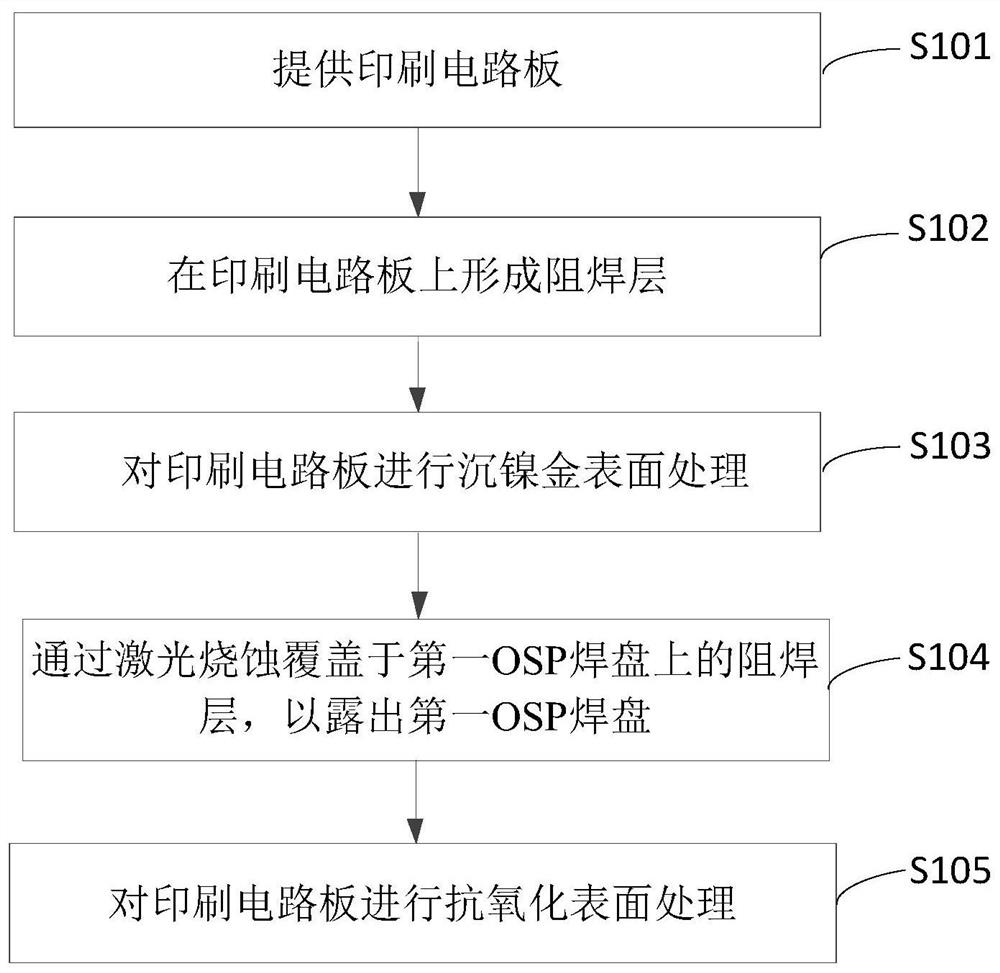
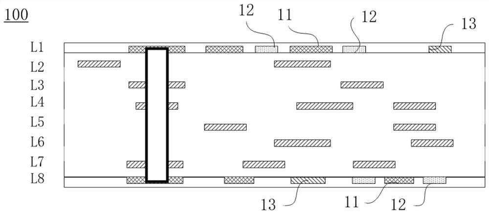
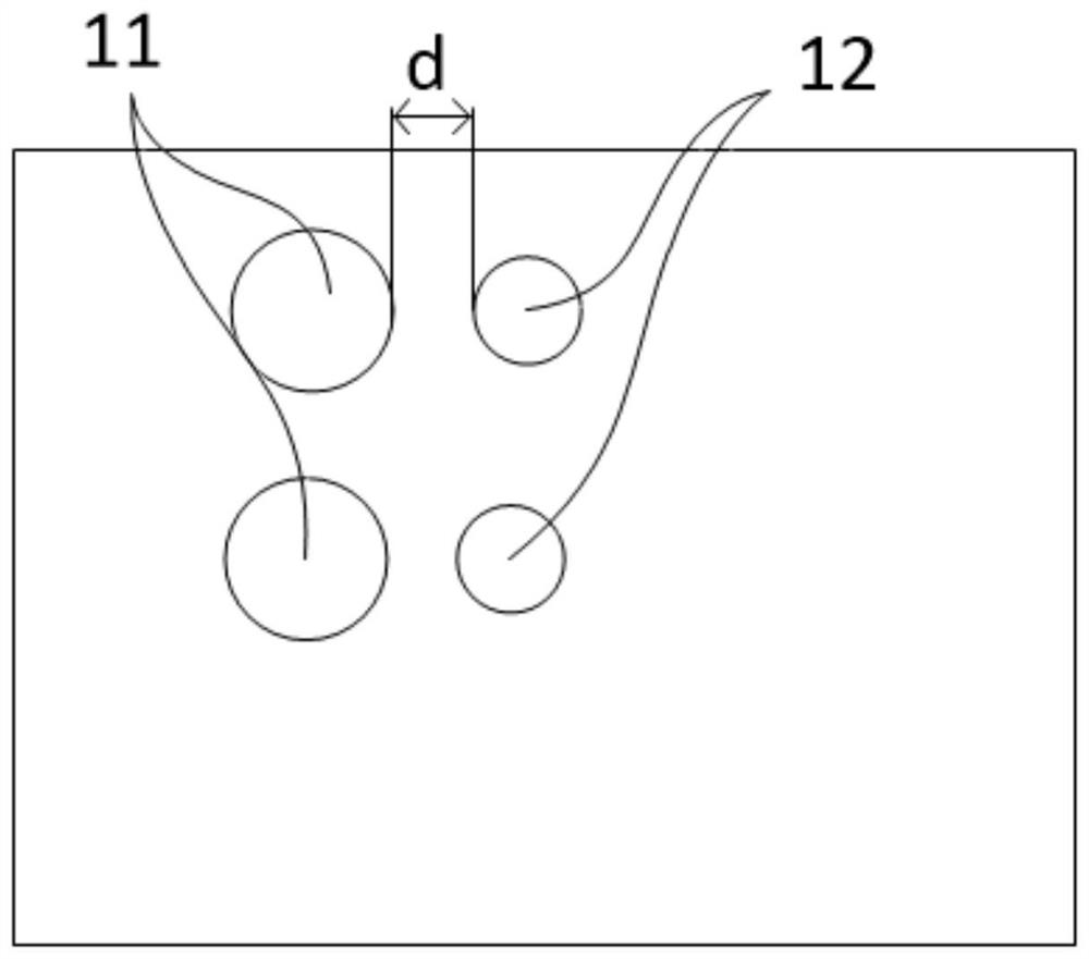
[0030] In order to make the object, technical solution and advantages of the present invention clearer, the present invention will be further described in detail below in conjunction with the accompanying drawings, that is, embodiments. It should be understood that the specific embodiments described here are only used to explain the present invention, not to limit the present invention.

[0031] It should be noted that when a component is referred to as being “fixed on” or “disposed on” another component, it may be directly or indirectly on the other component. When an element is referred to as being "connected to" another element, it can be directly or indirectly connected to the other element. The orientation or positional relationship indicated by the terms "upper", "lower", "left", "right", etc. are based on the orientation or positional relationship shown in the drawings, and are for convenience of description only, rather than indicating or implying the referred device ...


PUM


Abstract

The invention is suitable for the technical field of printed circuit boards, and provides a surface treatment method of a printed circuit board, which comprises the following steps: providing a printed circuit board, the printed circuit board comprising an outer layer circuit pattern, and the outer layer circuit pattern comprising an electroless nickel immersion gold (ENIG) pad and a first OSP pad; forming a solder mask layer on the printed circuit board, wherein the solder mask layer covers the first OSP bonding pad and exposes the ENIG pad; performing ENIG surface treatment on the printed circuit board; ablating the solder mask layer covering the first OSP bonding pad through laser so as to expose the first OSP bonding pad; and carrying out anti-oxidation surface treatment on the printed circuit board. According to the surface treatment method of the printed circuit board, ENIG treatment and anti-oxidation mixed surface treatment can be carried out on the printed circuit board with relatively high integration level, and the production efficiency is relatively high. The invention further provides a printed circuit board.

Description

technical field [0001] The invention relates to the technical field of printed circuit boards, in particular to a method for surface treatment of printed circuit boards and the printed circuit board. Background technique [0002] Surface treatment is an important process in the manufacturing process of Printed Circuit Board (PCB), which is used to make a layer of protection on the copper surface of the printed circuit board, which is beneficial to improve the electrical performance and reliability of the printed circuit board. [0003] Common surface treatment methods include Immersion Gold (Immersion Gold), anti-oxidation (Organic Solderability Preservatives, OSP), etc. For pads that do not need to mount components, you can choose to use immersion nickel gold surface treatment to enhance oxidation resistance, but its disadvantage is that the price and cost are relatively high, while OSP treatment has good soldering performance and is the main choice for high-density circuit...

Claims


Application Information

Patent Timeline
IPC IPC(8): H05K3/22H05K3/28
CPCH05K3/22H05K3/28H05K3/288
Inventor 白亚旭吴永恒焦鹏云王俊
Owner SHENZHEN KINWONG ELECTRONICS
Why Eureka
Try Eureka