Non-contact cleaning device for surfaces of PCBs

A technology for PCB boards and cleaning devices, applied in measurement devices, cleaning methods and appliances, cleaning methods using gas flow, etc., can solve problems such as poor cleaning, easy existence of dead corners, and many components, and improve test accuracy. The effect of reducing poor contact and improving cleanability

Active Publication Date: 2021-07-23
苏州凌创科技发展有限公司
View PDF11 Cites 6 Cited by
  • Summary
  • Abstract
  • Description
  • Claims
  • Application Information

AI Technical Summary

Problems solved by technology

[0007] Aiming at the problems in the prior art, the object of the present invention is to provide a non-contact cleaning device for the surface of the PCB, which solves the problem of simultaneously cleaning 12 There are no successful cases for reference, and its process characteristics are as follows: 1. It is usually difficult to transport 12 PCB boards at the same time; 2. The materials to be cleaned are complex and have many components; 3. The cleaning space is narrow , Crowded, manual cleaning is not easy, and technical problems are likely to exist in dead corners

Method used


Image

  • Non-contact cleaning device for surfaces of PCBs
  • Non-contact cleaning device for surfaces of PCBs
  • Non-contact cleaning device for surfaces of PCBs

Examples


Embodiment 1

[0061] see figure 1 , figure 2 , image 3 , Figure 4 and Figure 5 , is a schematic diagram of the entire structure of a PCB board multi-test process integrated test production line.

[0062] Among them, see figure 1 and figure 2 , an integrated test production line with multiple test procedures for PCB boards, including a No. 1 assembly line rack 1, a No. 2 assembly line rack 7 arranged side by side on the No. 1 assembly line rack 1, and the top of the No. 1 assembly line rack 1 The surface is a horizontal plane, the middle part of the top of the No. 1 assembly line frame 1 is an empty structure, the front and rear sides of the top of the No. 1 assembly line frame 1 are symmetrically provided with the No. 1 conveyor belt 2, and the top of the No. 1 assembly line frame 1 is placed. There are several PCB boards arranged in a matrix at equal intervals on the top of the pallet 6. The pallet 6 is placed on the No. 1 conveyor belt 2 on the front and rear sides of the top o...

Embodiment 2

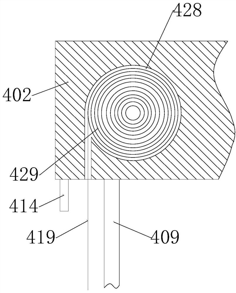
[0096] see figure 1 , figure 2 as well as Figure 6-Figure 14 , this embodiment has similarities with the above-mentioned embodiment 1, and the similarities will not be repeated in this embodiment, and the specific differences are:

[0097] The PCB board non-contact cleaning device includes No. 1 assembly line rack 1 and No. 2 assembly line rack 7 arranged side by side on No. 1 assembly line rack 1. The top surface of No. 1 assembly line rack 1 is a horizontal plane. The middle part of the top of the assembly line frame 1 is an empty structure, the front and rear sides of the top of the No. 1 assembly line frame 1 are symmetrically provided with the No. 1 conveyor belt 2, and the top of the No. 1 assembly line frame 1 is placed with a supporting plate 6, and the tops of the supporting plates 6 are equally spaced There are several PCB boards arranged in a matrix, and the pallet 6 is placed on the No. 1 conveyor belt 2 on the front and rear sides of the top of the No. 1 assem...

Embodiment 3

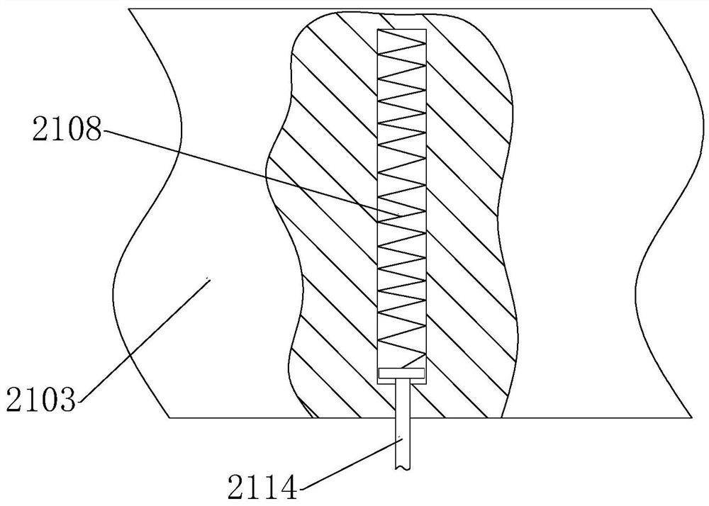
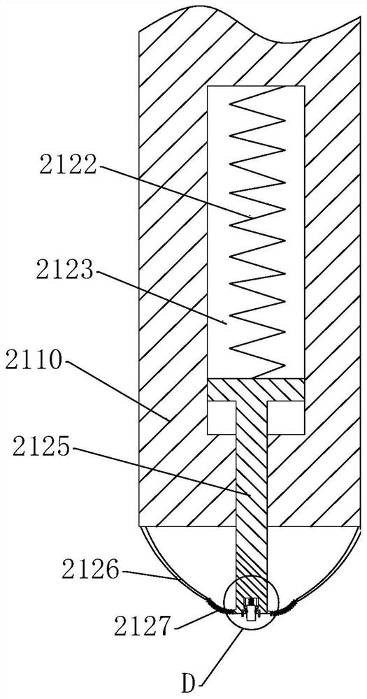
[0125] see figure 1 , figure 2 as well as Figure 15-Figure 23 , this embodiment has similarities with the above-mentioned embodiment 1, and the similarities will not be repeated in this embodiment, and the specific differences are:

[0126] The multiple groups of PCB board floating test devices include No. 1 assembly line frame 1, and No. 2 assembly line frame 7 arranged side by side on No. 1 assembly line frame 1. The top surface of No. 1 assembly line frame 1 is a horizontal plane. The middle part of the top of the No. 1 assembly line frame 1 is an empty structure, and the front and rear sides of the top of the No. 1 assembly line frame 1 are symmetrically provided with the No. 1 conveyor belt 2, and the top of the No. 1 assembly line frame 1 is placed with a pallet 6, the top of the pallet 6, etc. There are several PCB boards arranged in a matrix according to the spacing, and the pallet 6 is placed on the No. 1 conveyor belt 2 on the front and rear sides of the top of t...


PUM


Abstract

The invention provides a non-contact cleaning device for surfaces of PCBs, and relates to the technical field of PCB testing and processing. The device comprises a No.1 assembly line rack and a No.2 assembly line rack arranged on the side edge of the No.1 assembly line rack in parallel, wherein the top end face of the No.1 assembly line rack is a horizontal plane, the middle of the top end of the No.1 assembly line rack is of a hollow structure, No.1 conveying belts are symmetrically arranged on the front side and the rear side of the top end of the No.1 assembly line rack, a supporting plate is placed at the top end of the No.1 assembly line rack, and a plurality of PCBs are arranged at the top end of the supporting plate at equal intervals in a matrix mode. According to the non-contact cleaning device for the surfaces of the PCBs, the PCBs can be effectively prevented from floating when a blowing device I and a blowing device II blow typhoon to the surfaces of the PCBs, and dust blown out by the blowing device I and the blowing device II enters an explosion-proof filtering system through an air suction pipeline. The explosion-proof filtering system filters the dust cleaned from the PCBs, so that the toxicity of the dust adsorbed on the surfaces of the PCBs is reduced. The non-contact cleaning of the PCBs is realized.

Description

technical field [0001] The invention relates to the technical field of PCB board testing and processing, in particular to a non-contact cleaning device for the surface of a PCB board. Background technique [0002] In the process of using the PCB board production line, it is necessary to perform a programming program on the PCB board to verify whether the produced PCB can be used normally. In the existing process of testing the PCB board, it is necessary to test the PCB board at different equipment stations. For program processing, if it is necessary to clean and remove the dust on the surface of the PCB board first, then install the PCB board on the pallet for testing. Therefore, during the testing process of the PCB board, it is necessary to switch between the PCB boards at different equipment stations location, this process takes up the time efficiency of the production line body. [0003] At present, in the process of cleaning and dedusting the surface of PCB boards, in ...

Claims


Application Information

Patent Timeline
Patent Type & Authority Applications(China)
IPC IPC(8): B08B5/02B08B15/04B08B13/00G01R31/01G01R31/28
CPCB08B5/02B08B15/04B08B13/00G01R31/01G01R31/2806
Inventor 张云龙于贵伟黄春雷干恩
Owner 苏州凌创科技发展有限公司
Why Eureka
Try Eureka