Supercharge Your Innovation With Domain-Expert AI Agents!

Capacitive coupling in a direct-bonded interface for microelectronic devices

A microelectronic device, capacitive coupling technology, applied in the direction of electric solid-state devices, electrical components, semiconductor devices, etc., can solve the problem of relying on discrete capacitors

Pending Publication Date: 2021-07-23
INVENSAS CORP
View PDF10 Cites 0 Cited by
  • Summary
  • Abstract
  • Description
  • Claims
  • Application Information

AI Technical Summary

Problems solved by technology

[0004] In addition, the size reduction of wafer-level packages and microelectronics is sometimes inhibited by the necessary inclusion of difficult-to-miniaturize components
For example, sometimes packages rely on the relatively large size of discrete capacitors

Method used


Image

  • Capacitive coupling in a direct-bonded interface for microelectronic devices
  • Capacitive coupling in a direct-bonded interface for microelectronic devices
  • Capacitive coupling in a direct-bonded interface for microelectronic devices

Examples


Embodiment Construction

[0019] overview

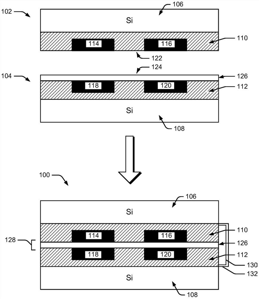
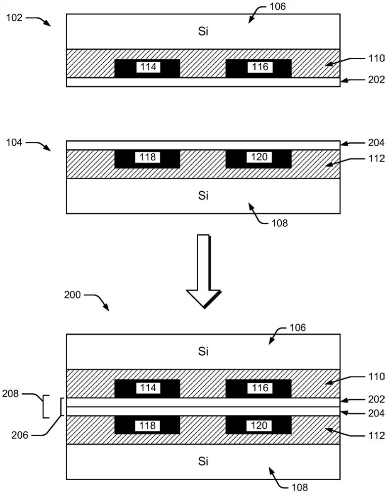
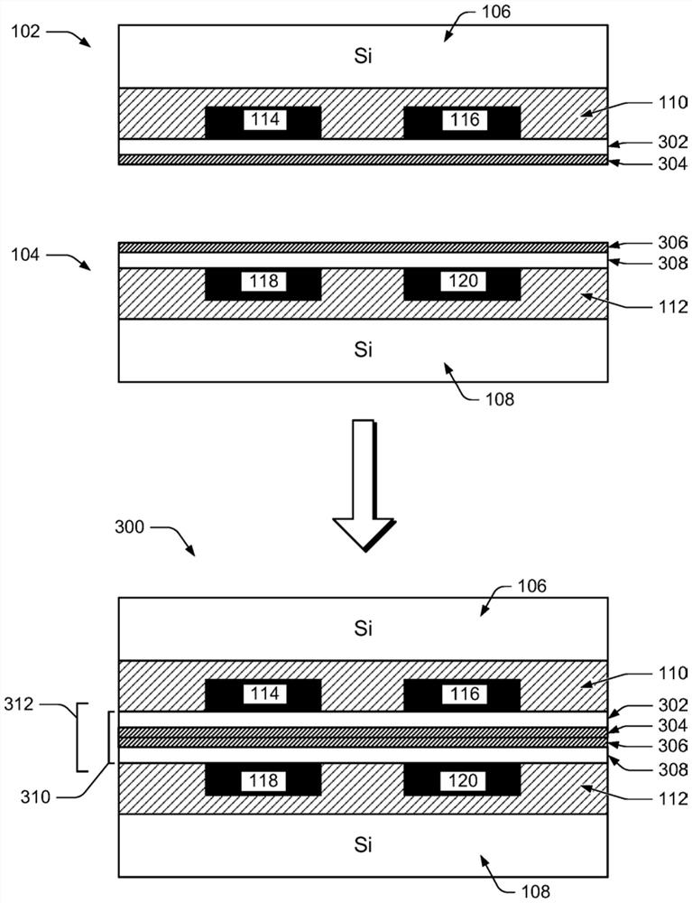
[0020] The present disclosure describes capacitive coupling in interfaces for direct bonding of microelectronic devices. The direct hybrid bonding process used for microelectronic dies and wafers also creates capacitive coupling for each individual signal line at the bonding interface. In one embodiment, the direct hybrid bonding process produces a direct bond between the dielectric surfaces of the two dies, a direct bond between the corresponding power interconnects of the two dies, and a direct bond between the corresponding ground interconnects of the two dies. Direct bonding occurs between interconnects and capacitive coupling occurs for each signal line at the bonding interface of the direct hybrid bonding process.

[0021] The direct bonding between the dielectric surfaces may be an oxide-oxide direct bonding. The direct bond between the corresponding power interconnects is a direct metal-to-metal bond. A direct bond between corresponding ground inte...


PUM

PropertyMeasurementUnit
Thicknessaaaaaaaaaa
Thicknessaaaaaaaaaa

Abstract

Capacitive couplings in a direct- bonded interface for microelectronic devices are provided. In an implementation, a microelectronic device includes a first die and a second die direct bonded together at a bonding interface, a conductive interconnect between the first die and the second die formed at the bonding interface by a metal-to-metal direct bond, and a capacitive interconnect between the first die and the second die formed at the bonding interface. A direct bonding process creates a direct bond between dielectric surfaces of two dies, a direct bond between respective conductive interconnects of the two dies, and a capacitive coupling between the two dies at the bonding interface. In an implementation, a capacitive coupling of each signal line at the bonding interface comprises a dielectric material forming a capacitor at the bonding interface for each signal line. The capacitive couplings result from the same direct bonding process that creates the conductive interconnects direct- bonded together at the same bonding interface.

Description

[0001] Cross References to Related Applications [0002] This application claims the benefit of priority to U.S. Patent Application Serial No. 16 / 212,248, filed December 6, 2018, which is an extension of Application Serial No. 16 / 020,654, filed June 27, 2018 Continuation-in-Part of Application No. 16 / 020,654 of U.S. Patent Application No. 15 filed August 25, 2016 claiming the benefit of priority to U.S. Provisional Patent Application No. 62 / 234,022, filed September 28, 2015 / 247,705 (now U.S. Patent No. 10,032,751, published July 24, 2018), all of which are hereby incorporated by reference in their entirety. Background technique [0003] Direct and direct hybrid joints sometimes require critical tolerances. These processes can become more forgiving when various ways of coupling power, ground, and signal lines at the bonding interface can be designed, for example, allowing for some misalignment and allowing for lower critical tolerances in order to Bonding yield provides a m...

Claims


Application Information

Patent Timeline
IPC IPC(8): H01L25/065H01L25/00H01L23/00H01L21/311H01L21/02
CPCH01L24/80H01L25/0657H01L23/5223H01L2225/06531H01L2225/06541H01L2225/06565H01L2224/08145H01L2224/80895H01L2224/80896H01L2224/8089H01L2224/034H01L2224/03602H01L2224/0361H01L2224/06505H01L2224/09051H01L2224/09505H01L2224/06051H01L2224/0603H01L24/08H01L24/09H01L24/05H01L24/06H01L25/50H01L2224/051H01L2224/056H01L2224/05186H01L2224/05686H01L2224/05695H01L2224/0569H01L2224/80379H01L2224/08121H01L2224/80365H01L2224/80357H01L2924/00012H01L2924/00014H01L2924/05442H01L2924/05432H01L2924/06H01L2924/05042H01L2924/0534H01L2924/0544
Inventor B·哈巴A·R·西塔拉姆
Owner INVENSAS CORP
Features
  • R&D
  • Intellectual Property
  • Life Sciences
  • Materials
  • Tech Scout
  • Unparalleled Data Quality
  • Higher Quality Content
  • 60% Fewer Hallucinations
Learn More