Gate driver with CMOS structure
A gate driver and gate technology, which is applied in the direction of output power conversion devices, electrical components, electronic switches, etc., to achieve the effect of lowering the possibility of through-current and reducing power consumption
- Summary
- Abstract
- Description
- Claims
- Application Information
AI Technical Summary
Problems solved by technology
Method used
Image

Examples
Embodiment 1
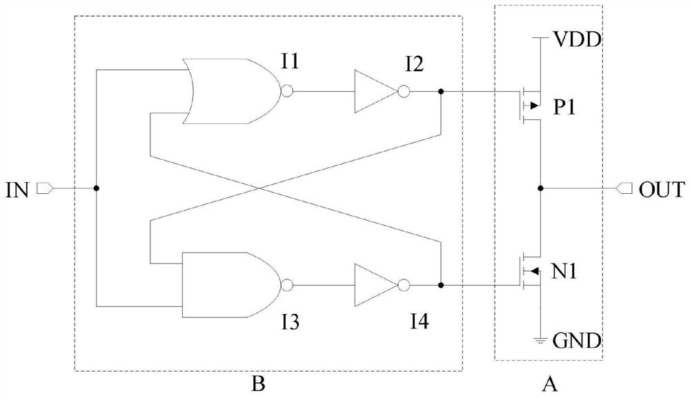
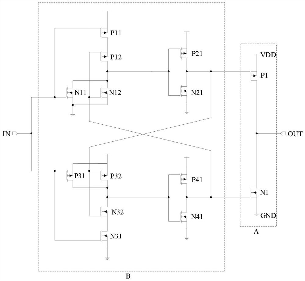
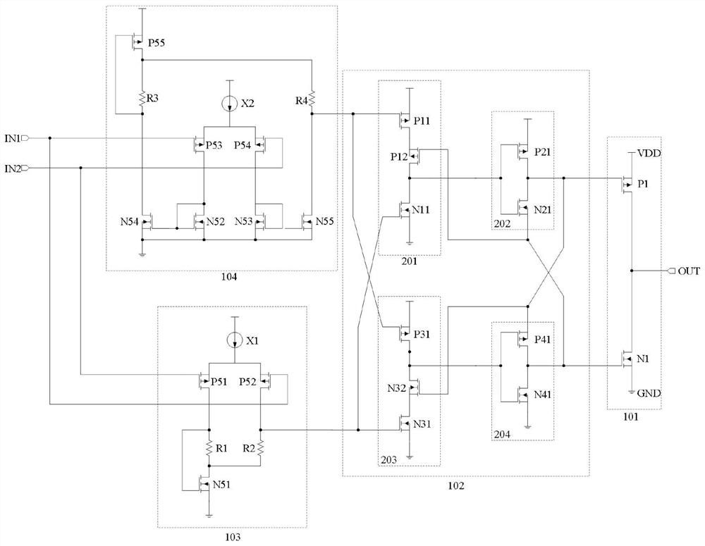
[0047] The present invention provides a gate driver with a CMOS structure, the structure of which is as follows image 3 As shown, it includes an output driver stage 101 , a dead time control circuit 102 , an NMOS control circuit 103 and a PMOS control circuit 104 . The output driver stage 101 is used to drive an external power switch tube. The output driver stage 101 includes a PMOS transistor P1 and an NMOS transistor N1. The drain of the PMOS transistor P1 is connected to the drain of the NMOS transistor N1 as an output terminal of the CMOS driver. OUT; the dead time control circuit 102 controls the output driver stage 101, and generates a dead time to reduce the possibility of output driver stage 101 breakthrough, and the dead time control circuit 102 includes a first logic unit 201, a second A logic unit 202, a third logic unit 203, and a fourth logic unit 204; the second logic unit 202 is connected to the gate of the PMOS transistor P1, and the fourth logic unit 204 is c...
PUM
 Abstract
Description
Claims
Application Information
 - R&D
- Intellectual Property
- Life Sciences
- Materials
- Tech Scout
- Unparalleled Data Quality
- Higher Quality Content
- 60% Fewer Hallucinations
Browse by: Latest US Patents, China's latest patents, Technical Efficacy Thesaurus, Application Domain, Technology Topic, Popular Technical Reports.
© 2025 PatSnap. All rights reserved.Legal|Privacy policy|Modern Slavery Act Transparency Statement|Sitemap|About US| Contact US: help@patsnap.com