Integrated circuit structure and memory

A technology of integrated circuits and circuit areas, applied in static memory, instruments, etc., can solve the problems of large tDQS2DQ value, temperature and voltage interference, etc.

Pending Publication Date: 2021-07-30
CHANGXIN MEMORY TECH (SHANGHAI) INC
0 Cites 1 Cited by

AI-Extracted Technical Summary

Problems solved by technology

[0007] The purpose of the present disclosure is to provide an integrated circuit structure and memory, and then at least to a certain extent overcome the problems of l...

Abstract

The invention provides an integrated circuit structure and a memory, and relates to the technical field of semiconductor memories. The integrated circuit structure includes: a pad region including a plurality of signal pads arranged in a target direction; the first circuit area that is arranged on one side of the bonding pad area and comprises a plurality of signal input circuit modules which are arranged in the target direction and correspondingly connected with the signal bonding pads, and the signal input circuit modules are used for achieving sampling operation of input signals and writing sampling results into a storage array, wherein the size of the first circuit area along the target direction is smaller than the size of the bonding pad area along the target direction. The performance of the write operation of the memory can be improved.

Application Domain

Static storage

Technology Topic

Integrated circuitEngineering +4

Image

  • Integrated circuit structure and memory
  • Integrated circuit structure and memory
  • Integrated circuit structure and memory

Examples

  • Experimental program(1)

Example Embodiment

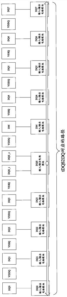
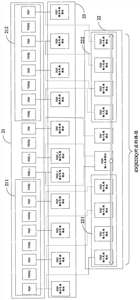
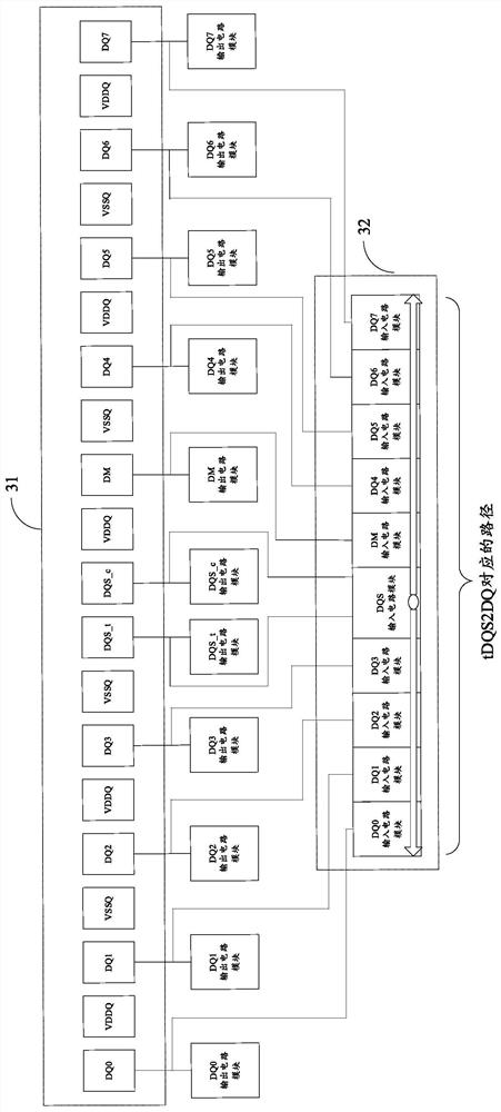
[0036] Example embodiments will now be described more fully with reference to the accompanying drawings. Example embodiments may, however, be embodied in many forms and should not be construed as limited to the examples set forth herein; rather, these embodiments are provided so that this disclosure will be thorough and complete and will fully convey the concept of example embodiments to those skilled in the art. The described features, structures, or characteristics may be combined in any suitable manner in one or more embodiments. In the following description, numerous specific details are provided in order to give a thorough understanding of embodiments of the present disclosure. However, those skilled in the art will appreciate that the technical solutions of the present disclosure may be practiced without one or more of the specific details being omitted, or other methods, components, devices, steps, etc. may be adopted. In other instances, well-known technical solutions have not been shown or described in detail to avoid obscuring aspects of the present disclosure.
[0037] Furthermore, the drawings are merely schematic illustrations of the present disclosure and are not necessarily drawn to scale. The same reference numerals in the drawings denote the same or similar parts, and thus repeated descriptions thereof will be omitted.
[0038] During the writing operation of the memory such as LPDDR4, the DQ input circuit module can obtain the signal transmitted by the DQ port, and this signal is often not a signal that can be directly processed by the digital circuit due to the influence of parasitic effects and various interferences. . In this case, the DQ input circuit module needs to use the DQS signal to sample the acquired DQ signal, and the DQ input circuit module writes the sampling result into the memory array.
[0039] Since the time taken by the DQS signal and the DQ signal to reach the LPDDR4 is almost the same, inside the LPDDR4, the DQS signal will take a while to be transmitted to the DQ input circuit module, which causes the DQS signal and the DQ signal to be out of sync. In order to avoid this situation, The chip of the semiconductor memory can send the DQS signal to the LPDDR4 by tDQS2DQ in advance, so that the DQS signal and the DQ signal can reach the DQ input circuit module synchronously, so as to improve the sampling accuracy of the DQ signal by the DQ input circuit module.
[0040] However, tDQS2DQ is easily affected by factors such as LPDDR4 internal operating voltage or operating temperature. In order to solve this problem, it is necessary to adjust tDQS2DQ by continuously detecting changes in internal operating voltage, operating temperature and other parameters, and the detection process consumes time and energy. This will slow down the writing speed and affect the working performance of the memory.
[0041] figure 1 Schematic diagrams showing integrated circuit structures for some technologies. In these technologies, since the DQ input/output circuit module and the signal pad are configured together during manufacture, the path for the acquired DQS signal to reach the DQ input/output circuit module at the two ends is relatively long, and the signal pad occupies a relatively long path. The length of the region is approximate. In the case of DQ including DQ0 to DQ7 with a total of 8 bits, if the corresponding signal pad pitch is 60 μm, then the sum of the paths of the DQS signal to the input/output circuit modules of DQ0 and DQ7 is about 1140 μm. In an exemplary embodiment of the present disclosure, the sum of the paths is recorded as a path corresponding to tDQS2DQ.
[0042] In view of this, if the path corresponding to tDQS2DQ is shortened, the influence of tDQS2DQ on operating voltage, operating temperature, etc. will also be reduced. In addition, shortening the path can also reduce current consumption and help ensure signal integrity. Thus, the writing performance of the memory can be improved.
[0043] The following will refer to figure 2 An integrated circuit structure of an exemplary embodiment of the present disclosure will be described.
[0044] refer to figure 2 , the integrated circuit structure may include a pad region 21 and a first circuit region 22 .
[0045] The pad area 21 includes a plurality of signal pads arranged along the target direction, wherein the signal pads refer to pads corresponding to each data signal port, which may include but not limited to a plurality of data input/output pads, first A differential data strobe pad, a second differential data strobe pad, and a data mask pad.
[0046] For multiple data input/output pads, take DQ including DQ0 to DQ7 for a total of 8 bits as an example, multiple data input/output pads include DQ0 pads, DQ1 pads, DQ2 pads, DQ3 pads, and DQ4 pads. pad, DQ5 pad, DQ6 pad, and DQ7 pad. However, it should be understood that, depending on the type of memory, the multiple data input/output pads may also include a total of 16 pads from DQ0 to DQ15 , which is not limited in the present disclosure.
[0047] The data input/output pad performs write and read operations in one. In the process of performing the write operation, the data input/output pad receives the data signal from the pin (pin) through the wire, and sends the data signal to the corresponding circuit module; in the process of performing the read operation, the data input/output pad The output pad receives the data signal from the corresponding circuit module, and sends the signal out through the pin.
[0048] As for the differential data strobe pads, in the memory above DDR4, it may include a first differential data strobe pad (marked as DQS_t pad) and a second differential data strobe pad (marked as DQS_c pad). The signal received by the first differential data strobe pad and the signal received by the second differential data strobe pad have the same amplitude and opposite phase. In the process of sampling by using the differential signal, the time point at which the two differential signals intersect may be, for example, the sampling time point, and the data signal is sampled accordingly.
[0049] For a data mask pad (DM pad), a mask signal for performing a partial write function may be input. When the received mask signal is low, the corresponding bit of the input data will be discarded.
[0050] In addition, the pad area 21 may also include a plurality of power pads (VDDQ pads) and a plurality of ground pads (VSSQ pads), for providing power and ground terminals.
[0051] According to an embodiment of the present disclosure, the pad region 21 may include a first pad subregion 211 and a second pad subregion 212 . The number of data input/output pads contained in the first pad sub-region 211 is the same as that contained in the second pad sub-region 212 , and both of them are half of the total number of data input/output pads. For example, the first pad sub-region 211 includes DQ0 pad, DQ1 pad, DQ2 pad and DQ3 pad, and the second pad sub-region 212 includes DQ4 pad, DQ5 pad, DQ6 pad and DQ7 pad.
[0052] In this case, the first differential data strobe pad, the second differential data strobe pad and the data mask pad can be arranged between the first pad sub-region 211 and the second pad sub-region 212 so that the differential It is easier for the data strobe signal to perform path matching on each DQ input circuit module, so as to avoid the problem of excessive distance difference.
[0053] It should be understood that, according to some other embodiments of the present disclosure, any one of the first differential data strobe pad, the second differential data strobe pad and the data mask pad can be arranged on the pad region 21 side, and its position relative to the respective data input/output pads is not restricted.
[0054] For the first circuit region 22 , it is disposed on one side of the pad region 21 , that is to say, the first circuit region 22 and the pad region 21 are two regions without overlapping regions. Corresponding to the multiple signal pads in the pad area 21 , the first circuit area 22 includes multiple signal input circuit modules arranged along the target direction, and each signal input circuit module is connected to the corresponding signal pads through metal wires. And each signal input circuit module is used to realize the sampling operation of the input signal, and write the sampling result into the memory array.
[0055] Wherein, the plurality of signal input circuit modules may include a plurality of data input circuit modules, data gating circuit modules and data mask circuit modules.
[0056] For multiple data input circuit modules, corresponding to the above multiple data input/output pads, the multiple data input circuit modules may include DQ0 input circuit module, DQ1 input circuit module, DQ2 input circuit module, DQ3 input circuit module, DQ4 Input circuit module, DQ5 input circuit module, DQ6 input circuit module and DQ7 input circuit module.
[0057] Each DQ input circuit module is used to receive the data signal sent by the corresponding DQ pad, and sample the data signal in response to the data strobe signal, so as to write the sampling result into the memory array.
[0058] For the data strobe circuit module, in the embodiments of the present disclosure, it can also be called a data strobe input circuit module, which is used to send the data strobe signal to each DQ input circuit module.
[0059] The data mask circuit module is used to obtain mask information and perform corresponding partial write operations.
[0060] According to an embodiment of the present disclosure, the first circuit area 22 includes a first circuit sub-area 221 and a second circuit sub-area 222 . The number of data input circuit modules contained in the first circuit sub-region 221 is the same as the number of data input circuit modules contained in the second circuit sub-region 222 , and both of them are half of the total number of data input circuit modules. For example, the first circuit sub-area 221 includes DQ0 input circuit module, DQ1 input circuit module, DQ2 input circuit module and DQ3 input circuit module, and the second circuit sub-area 222 includes DQ4 input circuit module, DQ5 input circuit module, DQ6 input circuit module and DQ7 input circuit modules.
[0061] In this case, the data gating circuit module and the data masking circuit module are arranged between the first circuit sub-region 221 and the second circuit sub-region 222 .
[0062] Also, refer to figure 2 , the data strobe circuit module can be connected to the first differential data strobe pad and the second differential data strobe pad through metal wires.
[0063] In an exemplary embodiment of the present disclosure, the size of the first circuit region 22 along the target direction is smaller than the size of the pad region 21 along the target direction. As mentioned above, the size of the first circuit region 22 along the target direction refers to the length of the first circuit region 22 along the direction of arranging a plurality of signal input circuit modules, that is, the path length corresponding to tDQS2DQ.
[0064] Configuring the size of the first circuit region 22 along the target direction to be smaller than the size of the pad region 21 along the target direction, on the one hand, reduces the path length for the DQS signal to be transmitted to the DQ input circuit module, thereby reducing tDQS2DQ; on the other hand On the one hand, a short path can reduce temperature and voltage interference, greatly improve temperature and voltage performance, and can also reduce current consumption, helping to ensure signal integrity, thereby improving memory performance.
[0065] According to some embodiments of the present disclosure, in the first circuit region 22 , the distance between adjacent signal input circuit modules is smaller than a distance threshold. Wherein, the distance threshold can be determined according to the size of the pad area 21 along the target direction and the size of each signal input circuit module along the target direction, so that the size of the first circuit area 22 along the target direction is smaller than that of the pad area 21 along the target direction. The dimension of the direction. It should be noted that the distances between adjacent signal input circuit modules may be the same or different.
[0066] like figure 2 As shown, there may be gaps between adjacent signal input circuit modules to avoid mutual interference between the modules.
[0067] In addition, the integrated circuit structure of the exemplary embodiment of the present disclosure further includes a second circuit region 23 .
[0068] The second circuit region 23 can be disposed on the same side as the first circuit region 22 relative to the pad region 21 , that is, relative to the pad region 21 , the first circuit region 22 and the second circuit region 23 are disposed on the same side. side.
[0069] The second circuit area 23 may include a plurality of signal output circuit modules arranged along the target direction, each signal output circuit module is connected to the corresponding signal pad through a metal wire, and each signal output circuit module is used to read out the data stored in the memory array .
[0070] In addition, the size of the first circuit region along the target direction can be set to be smaller.
[0071] refer to image 3 , pad area 31 with figure 2 The middle pad region 21 is the same, and will not be repeated here. For the first circuit region 32 , the distance between adjacent signal input circuit modules can be as small as possible, that is to say, the above-mentioned distance threshold can be configured to be as small as possible. like image 3 The configuration shown is a close-by structure, further shortening the path length corresponding to tDQS2DQ while saving more space in the manufacturing process.
[0072] Because the area of ​​the signal input circuit module is small, it is image 3 For the example structure shown, tDQS2DQ corresponds to a path of about 200 μm, compared to figure 1 1140 μm in some technologies, the path length is greatly reduced.
[0073] Also, refer to figure 2 or image 3 , in the embodiments of the present disclosure, the metal wires from the pads to the signal input circuit module can be configured to be very narrow, thereby not requiring large current driving and reducing the input capacitance.
[0074] The present disclosure also provides a memory, which includes any one of the integrated circuit structures described above.
[0075] It should be understood that the present disclosure does not limit the type of the memory, which may be, for example, DDR4 SDRAM of LPDDR4, or DDR5 memory.
[0076] Other embodiments of the disclosure will be readily apparent to those skilled in the art from consideration of the specification and practice of the invention disclosed herein. This application is intended to cover any modification, use or adaptation of the present disclosure, and these modifications, uses or adaptations follow the general principles of the present disclosure and include common knowledge or conventional technical means in the technical field not disclosed in the present disclosure . The specification and examples are to be considered exemplary only, with the true scope and spirit of the disclosure indicated by the appended claims.
[0077] It should be understood that the present disclosure is not limited to the precise constructions which have been described above and shown in the drawings, and various modifications and changes may be made without departing from the scope thereof. The scope of the present disclosure is limited only by the appended claims.

PUM

no PUM

Description & Claims & Application Information

We can also present the details of the Description, Claims and Application information to help users get a comprehensive understanding of the technical details of the patent, such as background art, summary of invention, brief description of drawings, description of embodiments, and other original content. On the other hand, users can also determine the specific scope of protection of the technology through the list of claims; as well as understand the changes in the life cycle of the technology with the presentation of the patent timeline. Login to view more.
Why Eureka
Try Eureka