Method for determining optimal read voltage of memory

A determination method and technology of reading voltage, applied in static memory, read-only memory, information storage and other directions, can solve the problems of many reading errors, data damage, exceeding the error correction capability of the error correction code of the control chip, etc. wrong effect

Active Publication Date: 2021-07-30
SHANDONG UNIV
View PDF4 Cites 1 Cited by
  • Summary
  • Abstract
  • Description
  • Claims
  • Application Information

AI Technical Summary

Problems solved by technology

If the default reading voltage is not adjusted, it may lead to more and more reading errors, exceeding the error correction capability of the error correction code of the control chip, resulting in data corruption

Method used


Image

  • Method for determining optimal read voltage of memory
  • Method for determining optimal read voltage of memory
  • Method for determining optimal read voltage of memory

Examples


Embodiment 1

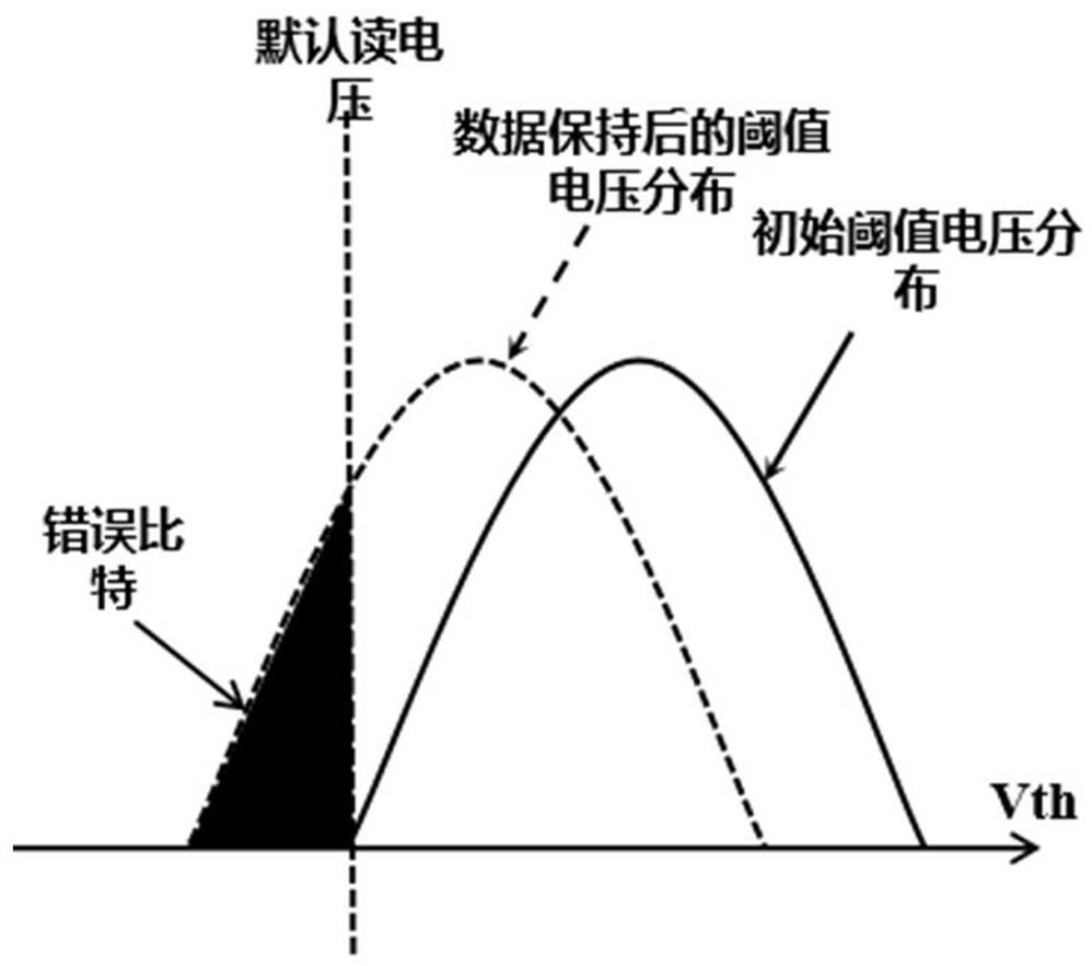
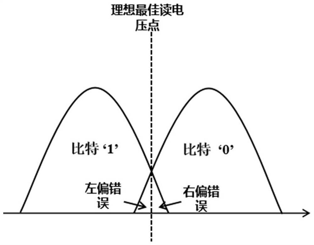
[0038] The threshold voltage distribution of NAND flash memory approximately conforms to the mathematical Gaussian function model. According to the mathematical relationship, it is easy to know that the ideal and optimal read voltage point is the intersection of adjacent threshold voltage states, such as image 3 shown. Among them, we call the bit error of writing data as '0' but reading it as '1' as left-bias error; the bit error of writing as '1' but reading as '0' is called right-bias error Bias error.

[0039] According to the error rules of NAND flash storage particles in the data retention scenario, this embodiment proposes a method for determining the optimal read voltage of the memory in combination with the variation of the threshold voltage and the Gaussian mathematical model. This method only needs to apply the default read voltage once to estimate the position of the optimal read voltage, and the deviation between the estimated optimal read voltage point and the i...


PUM


Abstract

The invention discloses a method for determining optimal read voltage of memory, which comprises the following steps of: firstly, setting an optimal read voltage point as an intersection point of adjacent threshold voltage states of a memory, and defaulting a read voltage point as a read voltage point set when the memory leaves a factory; and then calculating drift distances offset 1 and offset 2 of two adjacent threshold voltage states relative to the initial state, and an offset distance offset = (offset 1 + offset 2) / 2 of the optimal voltage reading point relative to the default voltage reading point, and determining the optimal voltage reading point according to the offset distance and the default voltage reading point. According to the method, the position of the optimal read voltage is determined through fewer read times, so that the read error of the memory is greatly reduced, and the efficiency and reliability of a memory system are improved.

Description

technical field [0001] The invention relates to the field of memory system controllers, in particular to a method for determining the optimum read voltage of a memory. Background technique [0002] The non-volatile memory market has experienced explosive growth over the past decade. NAND flash memory has become the mainstream storage medium in the field of non-volatile storage due to its good shock resistance, high integration density, low market price and excellent reliability performance. [0003] The main manifestations of NAND flash memory in the consumer market are: (1) SSD (Solid State Drive) for enterprise data centers, servers and personal computers; (2) UFS flash memory for mobile terminals such as tablets, mobile phones, and smart watches . Regardless of SSD or UFS flash memory, they are mainly composed of two parts: one is the storage particle, which provides the most basic storage function; the other is the control chip, which mainly controls, manages and optim...

Claims


Application Information

Patent Timeline
Patent Type & Authority Applications(China)
IPC IPC(8): G11C16/34G11C29/02G11C29/50
CPCG11C16/3404G11C29/028G11C29/50G11C2029/5004Y02D10/00
Inventor 陈杰智贾梦华
Owner SHANDONG UNIV
Why Eureka
Try Eureka